Timing diagrams, Capacitance – Rainbow Electronics DS3690 User Manual
Page 3
DS3690
3.3V 26-Channel, Three-Stateable
Transmission Gate
_______________________________________________________________________________________
3
Note 1: All voltages referenced to ground.
Note 2: Typical waveform shown is labeled CHxxA (input) to CHxxB (output), and is identical in function when selecting pin CHxxB
(as the input) to pin CHxxA (as the output).
Note 3: Output reference level is V
CC
/2.
Note 4: Input transitions prior to the CE falling edge are ignored (don’t care).
Note 5: Propagation delay differential between any two channels when using a common input signal source.
Note 6: Guaranteed by design and not 100% tested.
CAPACITANCE
(TA = +25°C)
PARAMETER SYMBOL
CONDITIONS
MIN
TYP
MAX
UNITS
Input Capacitance (CE) C
IN
Not production tested
5
pF
I/O Capacitance
C
IO
Not production tested
8
pF
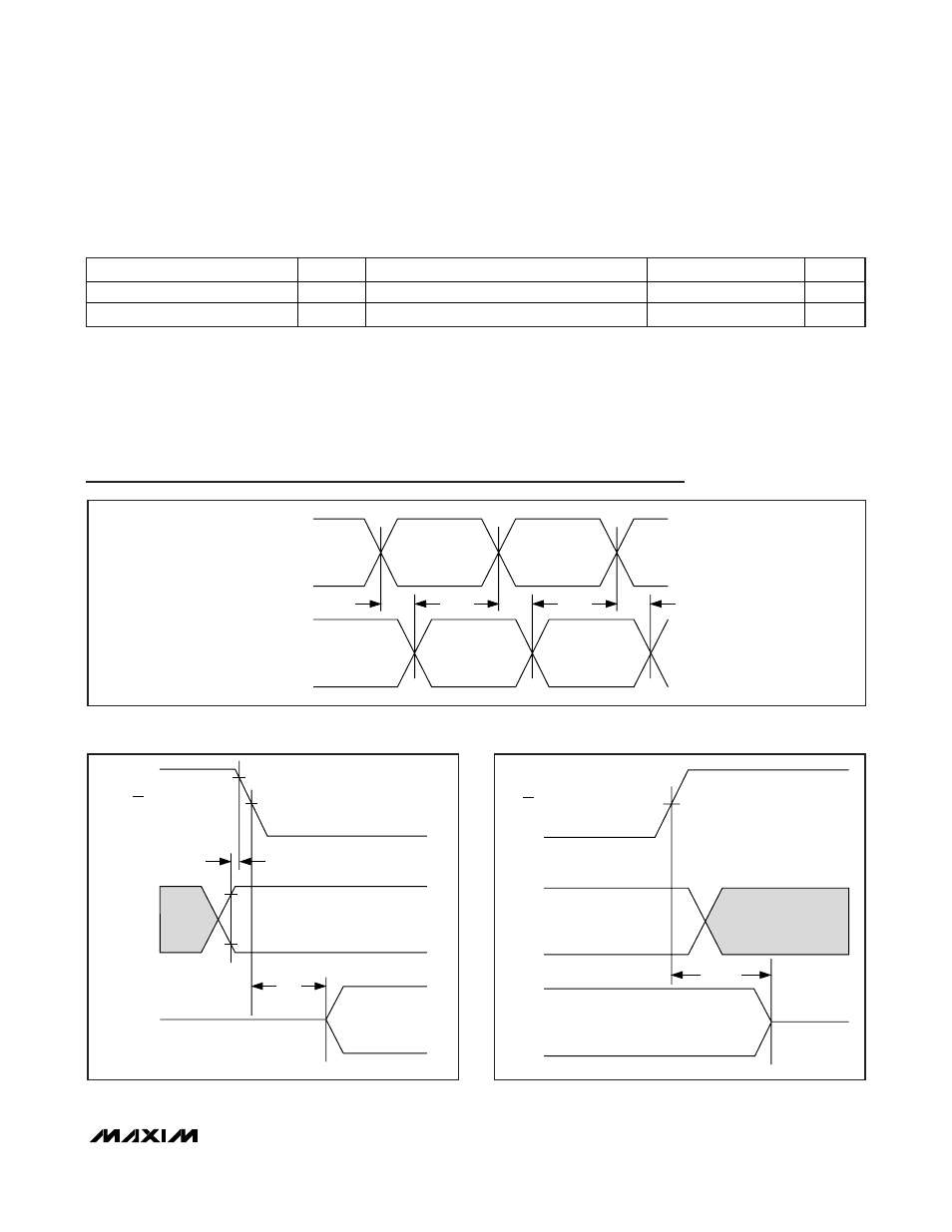
Timing Diagrams
CHxxA
CHxxB
t
PD
t
PD
t
PD
Figure 1. Digital Channel Propagation Delay
t
CEV
t
IS
HIGH IMPEDANCE
CHxxA
CHxxB
DON'T
CARE
CE
Figure 2. Digital Channels Enabled by CE
DON'T CARE
HIGH IMPEDANCE
CHxxA
CHxxB
CE
t
CEZ
Figure 3. Digital Channels Disabled by CE