Clock/calendar burst mode, Ram burst mode, Register summary – Rainbow Electronics DS1302 User Manual
Page 6
DS1302
6 of 15
DS1302 powers up with the trickle charger disabled. The diode select (DS) bits (bits 2–3) select whether
one diode or two diodes are connected between V
CC2
and V
CC1
. If DS is 01, one diode is selected or if DS
is 10, two diodes are selected. If DS is 00 or 11, the trickle charger is disabled independently of TCS.
The RS bits (bits 0–1) select the resistor that is connected between V
CC2
and V
CC1
. The resistor selected
by the resistor select (RS) bits is as follows:
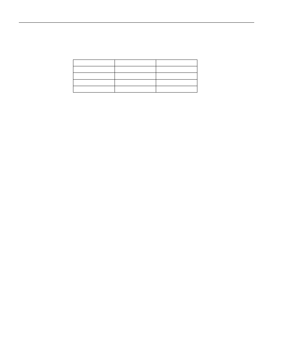
RS Bits
Resistor
Typical Value
00
None
None
01
R1
2kΩ
10
R2
4kΩ
11
R3
8kΩ
If RS is 00, the trickle charger is disabled independently of TCS.
Diode and resistor selection is determined by the user according to the maximum current desired for
battery or super cap charging. The maximum charging current can be calculated as illustrated in the
following example. Assume that a system power supply of 5V is applied to V
CC2
and a super cap is
connected to V
CC1
. Also assume that the trickle charger has been enabled with one diode and resistor R1
between V
CC2
and V
CC1
. The maximum current I
MAX
would, therefore, be calculated as follows:
I
MAX
= (5.0V - diode drop)/R1
» (5.0V - 0.7V) / 2kΩ » 2.2mA
As the super cap charges, the voltage drop between V
CC1
and V
CC2
will decrease and, therefore, the
charge current will decrease.
CLOCK/CALENDAR BURST MODE
The clock/calendar command byte specifies burst mode operation. In this mode the first eight
clock/calendar registers can be consecutively read or written (See Figure 4) starting with bit 0 of address
0.
If the write protect bit is set high when a write clock/calendar burst mode is specified, no data transfer
will occur to any of the eight clock/calendar registers (this includes the control register). The trickle
charger is not accessible in burst mode.
At the beginning of a clock burst read, the current time is transferred to a second set of registers. The
time information is read from these secondary registers, while the clock may continue to run. This
eliminates the need to re-read the registers in case of an update of the main registers during a read.
RAM
The static RAM is 31 x 8 bytes addressed consecutively in the RAM address space.
RAM BURST MODE
The RAM command byte specifies burst mode operation. In this mode, the 31 RAM registers can be
consecutively read or written (See Figure 4) starting with bit 0 of address 0.
REGISTER SUMMARY
A register data format summary is shown in Figure 4.