Operation – Rainbow Electronics DS1302 User Manual
Page 3
DS1302
3 of 15
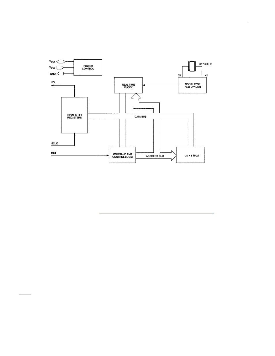
OPERATION
The main elements of the serial timekeeper (i.e., shift register, control logic, oscillator, RTC, and RAM)
are shown in Figure 1.
DS1302 BLOCK DIAGRAM Figure 1
SIGNAL DESCRIPTIONS
V
CC1
– V
CC1
provides low-power operation in single supply and battery-operated systems as well as low-
power battery backup. In systems using the trickle charger, the rechargeable energy source is connected
to this pin. UL recognized to ensure against reverse charging current when used in conjunction with a
lithium battery.
See “Conditions of Acceptability”
V
CC2
– V
CC2
is the primary power supply pin in a dual-supply configuration. V
CC1
is connected to a
backup source to maintain the time and date in the absence of primary power.
The DS1302 will operate from the larger of V
CC1
or V
CC2
. When V
CC2
is greater than V
CC1
+ 0.2V, V
CC2
will power the DS1302. When V
CC2
is less than V
CC1
, V
CC1
will power the DS1302.
SCLK (Serial Clock Input) – SCLK is used to synchronize data movement on the serial interface. This
pin has a 40kΩ internal pull-down resistor.
I/O (Data Input/Output) – The I/O pin is the bi-directional data pin for the 3-wire interface. This pin has
a 40kΩ internal pull-down resistor.
RST (Reset) – The reset signal must be asserted high during a read or a write. This pin has a 40kΩ
internal pull-down resistor.
X1, X2 – Connections for a standard 32.768kHz quartz crystal. The internal oscillator is designed for
operation with a crystal having a specified load capacitance of 6pF. For more information on crystal
selection and crystal layout considerations, please consult Application Note 58, “Crystal Considerations