Absolute maximum ratings, Electrical characteristics – Rainbow Electronics DS2784 User Manual
Page 2
DS2784: 1-Cell Stand-Alone Fuel Gauge IC with Li+ Protector and SHA-1 Authentication
2 of 38
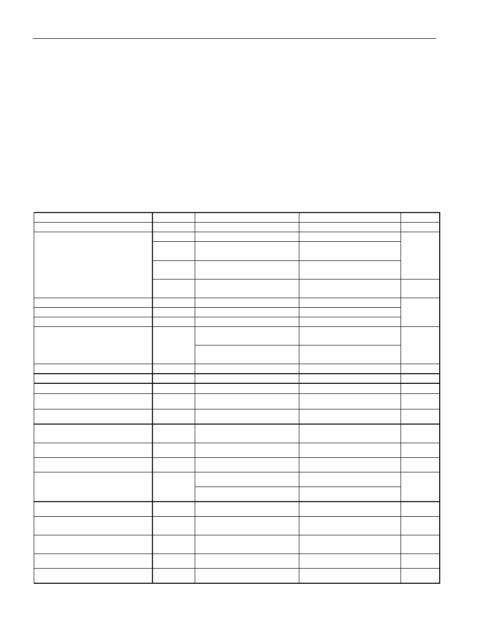
ABSOLUTE MAXIMUM RATINGS
Voltage Range on PLS Pin Relative to V
SS
-0.3V to +18V
Voltage Range on CP Pin Relative to V
SS
-0.3V to +12V
Voltage Range on DC Pin Relative to V
SS
-0.3V to (CP + 0.3V)
Voltage Range on CC Pin Relative to V
SS
V
DD
- 0.3V to CP + 0.3V
Voltage Range on All Other Pins Relative to V
SS
-0.3V to +6.0V
Maximum Voltage Range on V
IN
Pin Relative to V
DD
V
DD
+ 0.3V
Continuous Sink Current, PIO, DQ
20mA
Continuous Sink Current, CC, DC
10mA
Operating Temperature Range
-40°C to +85°C
Storage Temperature Range
-55°C to +125°C
Soldering Temperature (10s)
See IPC/JEDEC J-STD-020
*This is a stress rating only and functional operation of the device at these or any other conditions above those indicated in the operation
sections of this specification is not implied. Exposure to absolute maximum rating conditions for extended periods of time may affect reliability.
ELECTRICAL CHARACTERISTICS
(V
DD
= 2.5V to 4.6V, T
A
= -20
°C to +70°C, unless otherwise noted. Typical values are at T
A
= +25
°C.)
PARAMETER
SYMBOL CONDITIONS MIN
TYP
MAX
UNITS
Supply Voltage
V
DD
(Note 1)
2.5
4.6
V
I
DD0
Sleep mode
1
4
I
DD1
Sleep mode, V
DD
= 2.5V
0
°C to +50°C
0.4 1.5
I
DD2
Active mode
85
125
μA
Supply Current
I
DD3
Active mode during SHA
computation
300 500
μA
Temperature Accuracy
-3
+3
Temperature Resolution
0.125
Temperature Range
-128.000
+127.875
o
C
4.0 ≤ V
IN
≤ 4.6,
V
IN
≤ V
DD
+ 0.3V
-30 30
Voltage Accuracy, V
IN
2.5 ≤ V
IN
≤ 4.6V,
V
IN
≤ V
DD
+ 0.3V
-50 +50
mV
Voltage Resolution, V
IN
4.88
mV
Voltage Range, V
IN
0 4.99 V
Input Resistance, V
IN
15
M
Ω
Current Resolution
1.56
μV
Current Full Scale
-51.2
+51.2
mV
Current Gain Error
-1
+1
% full
scale
Current Offset
(Notes 2, 3, 4)
-15
+25
μV
Accumulated Current Offset
(Notes 2, 3, 4)
-360
0
μVh/day
0ºC ≤ T
A
≤ +50ºC
-2
+2
Time Base Error
-3
+3
%
CP Output Voltage
V
CP
I
CC
+ I
DC
= 0.9µA
8.50
9.25
10.00
V
CP Startup Time
t
SCP
CE = 0, DE = 0,
C
CP
= 0.1µF, Active mode
200 ms
Output High: CC, DC
V
OHCC
V
OHDC
I
OH
= -100µA (Note 5)
V
CP
- 0.4
V
Output Low: CC
V
OLCC
I
OL
= 100µA
V
DD
+ 0.1
V
Output Low: DC
V
OLDC
I
OL
= 100µA
0.1
V