Bit lasered rom code, Bit lasered rom code figure 5, Memory – Rainbow Electronics DS1822-PAR User Manual
Page 5: Ds1822-par memory map figure 6, Scratchpad (power-up state)
DS1822-PAR
5 of 19
64-BIT LASERED ROM CODE
Each DS1822-PAR contains a unique 64–bit code (see Figure 5) stored in ROM. The least significant 8
bits of the ROM code contain the DS1822-PAR’s 1–wire family code: 22h. The next 48 bits contain a
unique serial number. The most significant 8 bits contain a cyclic redundancy check (CRC) byte that is
calculated from the first 56 bits of the ROM code. A detailed explanation of the CRC bits is provided in
the CRC GENERATION section. The 64–bit ROM code and associated ROM function control logic
allow the DS1822-PAR to operate as a 1–wire device using the protocol detailed in the 1-WIRE BUS
SYSTEM section of this datasheet.
64-BIT LASERED ROM CODE Figure 5
8-BIT CRC
48-BIT SERIAL NUMBER
8-BIT FAMILY CODE (22h)
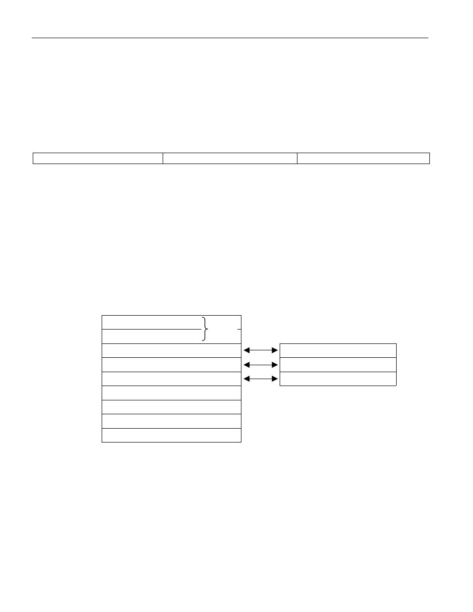
MEMORY
The DS1822-PAR’s memory is organized as shown in Figure 6. The memory consists of an SRAM
scratchpad with nonvolatile EEPROM storage for the high and low alarm trigger registers (T
H
and T
L
)
and configuration register. Note that if the DS1822-PAR alarm function is not used, the T
H
and T
L
registers can serve as general-purpose memory. All memory commands are described in detail in the
DS1822-PAR FUNCTION COMMANDS section.
DS1822-PAR MEMORY MAP
cáÖìêÉ=S
SCRATCHPAD (Power-up State)
byte 0 Temperature LSB (50h)
byte 1 Temperature MSB (05h)
EEPROM
byte 2 T
H
Register or User Byte 1*
T
H
Register or User Byte 1
byte 3 T
L
Register or User Byte 2*
T
L
Register or User Byte 2
byte 4 Configuration Register*
Configuration Register
byte 5 Reserved (FFh)
byte 6 Reserved (0Ch)
byte 7 Reserved (10h)
byte 8 CRC*
*
Power-up state depends on value(s) stored
in EEPROM
Byte 0 and byte 1 of the scratchpad contain the LSB and the MSB of the temperature register,
respectively. These bytes are read-only. Bytes 2 and 3 provide access to T
H
and T
L
registers. Byte 4
contains the configuration register data, which is explained in detail in the CONFIGURATION
REGISTER section of this datasheet. Bytes 5, 6 and 7 are reserved for internal use by the device and
cannot be overwritten; these bytes will return all 1s when read.
Byte 8 of the scratchpad is read-only and contains the cyclic redundancy check (CRC) code for bytes 0
through 7 of the scratchpad. The DS1822-PAR generates this CRC using the method described in the
CRC GENERATION section.
MSB MSB
LSB LSB
LSB
MSB
(85°C)