Rainbow Electronics BA6417F User Manual
Page 6
458
Motor driver ICs
BA6289F / BA6417F
(10) In-rush current
There are no circuits built into these ICs that prevent in-
rush currents. Therefore, it is recommended to place a
current limiting resistor or other physical countermea-
sure.
(11) Factors regarding the thermal, power supply, and
motor conditions
If the potential of the output pin sways greatly and goes
below the potential of ground, the operation of the IC may
malfunction or be adversely affected. In such a case,
place a diode between the output and ground, or other
measure, to prevent this.
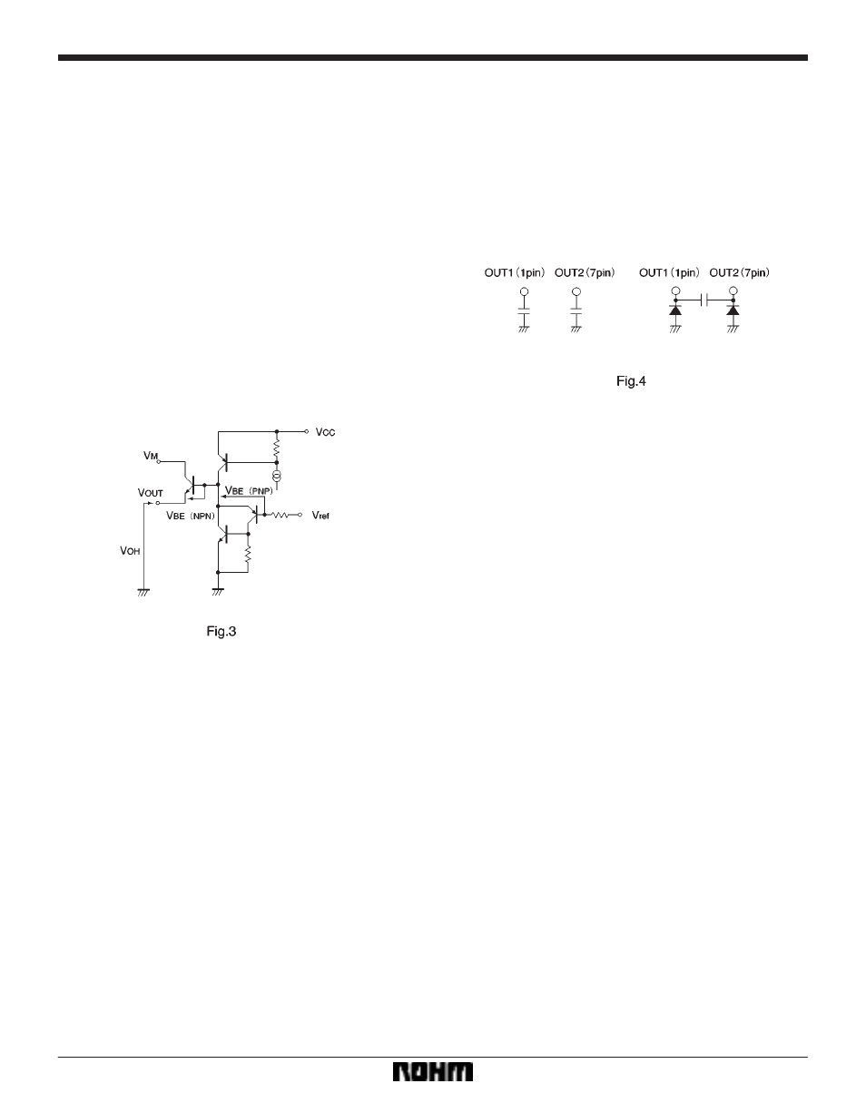
(12) HIGH level output voltage setting pin
The output voltage can be varied by controlling the V
ref
voltage :
V
OH
=V
ref
+V
BE
(PNP)–V
BE
(NPN)+(V
OUT
–V
ref
offset)
The voltage applied to the V
ref
pin should not exceed the
motor supply voltage (pin 2) or the V
CC
voltage. The V
ref
input range over which the HIGH level output voltage can
be controlled according to the above equation is between
0V and (V
CC
–V
SAT
–V
BE
).
The output may oscillate if the V
ref
voltage is controlled by
a low-impedance circuit. Set the voltage by either provid-
ing an impedance of about 10k
Ω
or connecting a capaci-
tor between the V
ref
and GND pins. Because the optimum
impedance and capacitance values depend on such fac-
tors as the type of motor, the PCB pattern, and the load
current, the values must be determined separately for
each application.
(13) Thermal shutdown circuit
When the thermal shutdown circuit is activated at the IC
junction temperature of about 175
_
C (typical), all driver
outputs are turned OFF. There is a temperature differ-
ence of about 15
_
C (typical) between the temperatures
at which the circuit is activated and deactivated.
(13) The input pins (pins 4 and 5 have temperature de-
pendent characteristics. Take the temperature effect into
consideration when using the IC.
(14) To eliminate motor noise, connect a capacitor be-
tween OUT1 (pin 1) and GND and between OUT2 (pin 7)
and GND. Alternatively, connect a capacitor between
OUT1 and OUT2, and also a diode between OUT1 and
GND and between OUT2 and GND.