Pin description – Rainbow Electronics DS8314 User Manual
Page 7
DS8313/DS8314
Smart Card Interface
_______________________________________________________________________________________
7
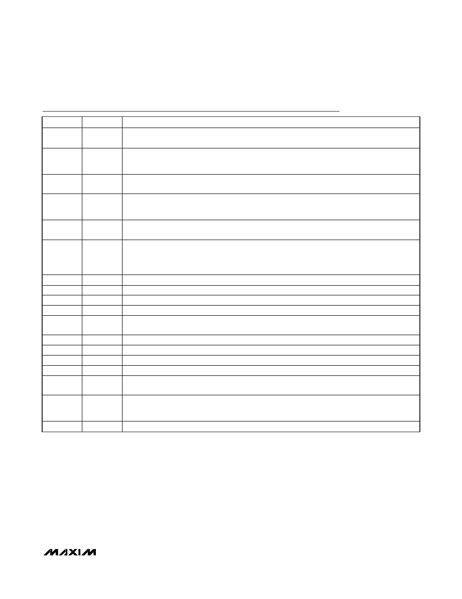
Pin Description
PIN
NAME
FUNCTION
1, 2
CLKDIV1,
CLKDIV2
Clock Divider. Determines the divided-down input clock frequency (presented at XTAL1 or from a
crystal at XTAL1 and XTAL2) on the CLK output pin. Dividers of 1, 2, 4, and 8 are available.
3 5V/3V
5V/3V Selection Pin. Allows selection of 5V or 3V for communication with an IC card. Logic-high
selects 5V operation; logic-low selects 3V operation. The 1_8V pin overrides the setting on this pin if
active. See Table 3 for a complete description of choosing card voltages.
4 1_8V
1.8V Operation Selection. Active-high selection for 1.8V smart card communication. An active-high
signal on this pin overrides any setting on the 5V/3V pin.
5, 7, 8, 9,
12, 13, 27,
28
N.C.
No Connection/Don’t Care. These pins are not bonded out.
6, 18
V
DDA
(N.C.)
Analog (Smart Card) Supply. Connect to 5V power supply. Pin 18 is N.C. for the DS8314.
10 PRES
Card Presence Indicator. Active-high card presence input from the DS8313 to the microcontroller.
When the presence indicator becomes active, a debounce timeout begins. After 8ms (typ), the OFF
signal becomes active. A trim optim defines whether or not the part provides active-low presence
detection.
11
I/O
Smart Card Data-Line Output. Card data communication line, contact C7.
14 CGND
Smart
Card
Ground
15
CLK
Smart Card Clock. Card clock, contact C3.
16
RST
Smart Card Reset. Card reset output from contact C2.
17 V
CC
Smart Card Supply Voltage. Decouple to CGND (card ground) with 2 x 100nF or 100 + 220nF
capacitors (ESR < 100m
).
19
CMDVCC
Activation Sequence Initiate. Active-low input from host.
20
RSTIN
Card Reset Input. Reset input from the host.
21 V
DD
Supply
Voltage
22 GND
Digital
Ground
23
OFF
Status Output. Active-low interrupt output to the host. Includes a 24k
integrated pullup resistor to
V
DD
.
24, 25
XTAL1,
XTAL2
Crystal/Clock Input. Connect an input from an external clock to XTAL1 or connect a crystal across
XTAL1 and XTAL2. For the low idle-mode current variant, an external clock must be driven on
XTAL1.
26
I/OIN
I/O Input. Host-to-interface chip data I/O line.