Read/write timing diagram (continued) figure 15, Program pulse – Rainbow Electronics DS2406 User Manual
Page 25
DS2406
25 of 31
READ/WRITE TIMING DIAGRAM (continued) Figure 15
Read-data Time Slot
RESISTOR
MASTER
DS2406
Master
Sampling Window
60 µs
£ t
SLOT
< 120 µs
1 µs
£ t
LOWR
< 15 µs
0
£ t
RELEASE
< 45 µs
1 µs
£ t
REC
<
¥
t
RDV
= 15 µs
t
SU
< 1 µs
V
PULLUP
V
PULLUP MIN
V
IH MIN
V
IL MAX
0V
t
SLOT
t
REC
t
LOWR
t
SU
t
RDV
t
RELEASE
* The optimal sampling point for the master is as close as possible to the end time of the 15
ms t
RDV
period without exceeding t
RDV
. For the case of a Read-one time slot, this maximizes the amount
of time for the pull-up resistor to recover the line to a high level. For a Read-zero time slot it
ensures that a read will occur before the fastest 1-Wire devices(s) release the line (t
RELEASE
= 0).
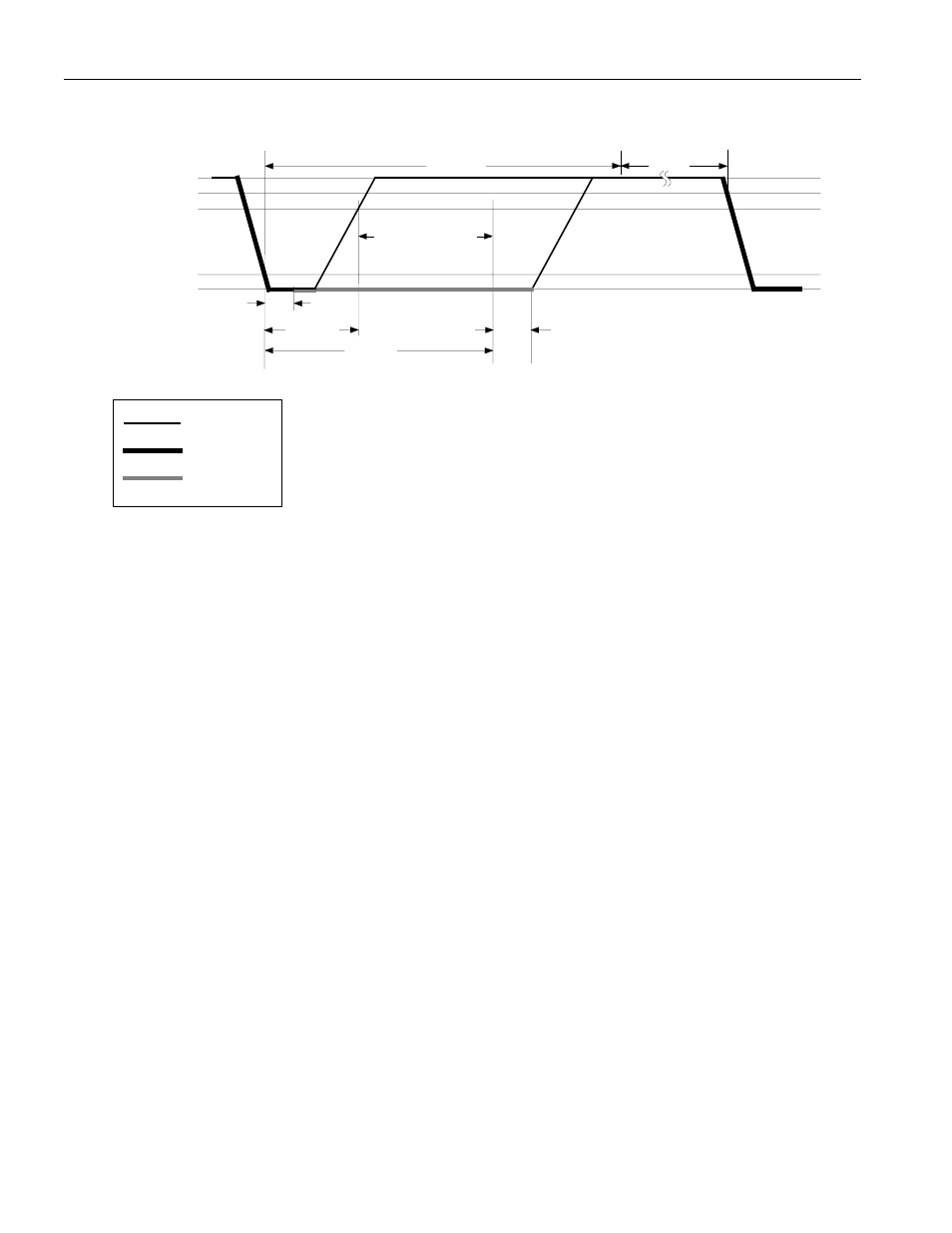
PROGRAM PULSE
To copy data from the 8-bit scratchpad to the EPROM data or status memory, a program pulse is applied
to the data line after the bus master has confirmed that the CRC for the current byte is correct. During
programming, the bus master controls the transition from a state where the data line is idling high via the
pull-up resistor to a state where the data line is actively driven to a programming voltage of 12V
providing a minimum of 10mA of current to the DS2406. This programming voltage (Figure 16) should
be applied for 480µs, after which the bus master should return the data line to the idle high state. Note
that due to the high voltage programming requirements for any 1-Wire EPROM device, it is not possible
to multi-drop non-EPROM based 1-Wire devices with the DS2406 during programming. An internal
diode within the non-EPROM based 1-Wire devices will attempt to clamp the data line at approximately
8V and could potentially damage these devices.