Pin description – Rainbow Electronics DS28EA00 User Manual
Page 4
DS28EA00 1-Wire Digital Thermometer with Sequence Detect and PIO
4 of 29
Note 18:
δ in Figure 14 represents the time required for the pullup circuitry to pull the voltage on IO up from V
IL
to the input high threshold
of the bus master. The actual maximum duration for the master to pull the line low is t
RLmax
+ t
F
Note 19:
This load current is caused by the internal weak pullup, which asserts a logic '1' to the PIOB and PIOA pins. The logical state of
PIOB must not change during the execution of the Conditional Read ROM command.
Note 20:
Current drawn from IO during EEPROM programming or temperature conversion interval in parasite powered mode. The pullup
circuit on IO during the programming or temperature conversion interval should be such that the voltage at IO is greater than or
equal to V
PUP(min)
. If V
PUP
in the system is close to V
PUP(min)
then a low impedance bypass of R
PUP
, which can be activated during
programming or temperature conversions may need to be added. The bypass must be activated within 10µs from the beginning
of the t
PROG
or t
CONV
interval, respectively.
Note 21:
The t
PROG
interval begins t
REHmax
after the trailing rising edge on IO for the last time slot of the command byte for a valid Copy
Scratchpad sequence. Interval ends once the device's self-timed EEPROM programming cycle is complete and the current
drawn by the device has returned from I
PROG
to I
L
(parasite power) or I
DDS
(local power).
Note 22:
Write-cycle endurance is degraded as T
A
increases.
Note 23:
Not 100% production-tested; guaranteed by reliability monitor sampling.
Note 24:
Data retention is degraded as T
A
increases.
Note 25:
Guaranteed by 100% production test at elevated temperature for a shorter time; equivalence of this production test to data sheet
limit at operating temperature range is established by reliability testing.
Note 26:
The t
CONV
interval begins t
REHmax
after the trailing rising edge on IO for the last time slot of the command byte for a valid Convert
Temperature sequence. Interval ends once the device's self-timed temperature conversion cycle is complete and the current
drawn by the device has returned from I
CONV
to I
L
(parasite power) or I
DDS
(local power).
Note 27:
Drift data is preliminary and based on a 1000-hour stress test performed on another device with comparable design and
fabricated in the same manufacturing process. This test was performed at greater than +85°C with V
DD
= 5.5V. Confirmed thermal
drift results for this device are pending the completion of a new 1000-hour stress test.
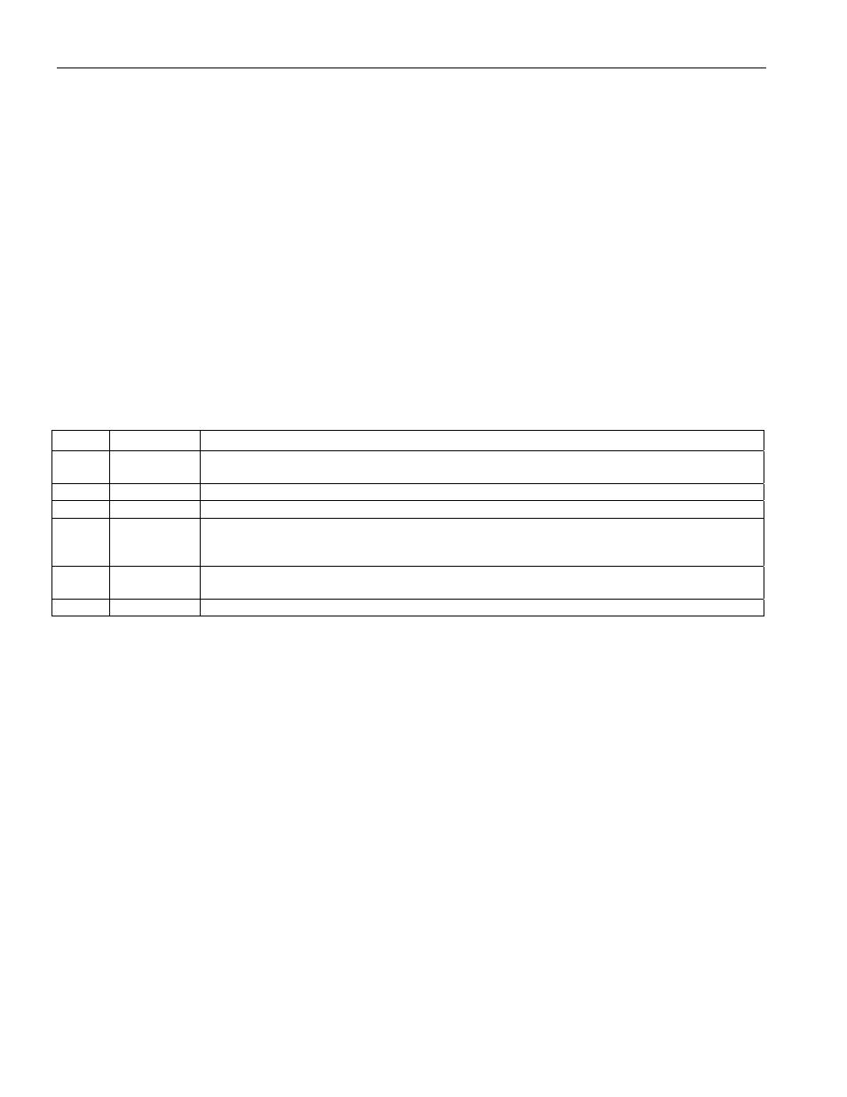
PIN DESCRIPTION
PIN NAME
FUNCTION
1 IO
1-Wire Bus Interface and Parasitic Power Supply. Open-drain, requires external pullup
resistor.
4 GND
Ground Supply
2, 3, 5
N.C. No
Connection
6
PIOA
(DONE\)
Open-Drain PIOA Channel and Chain Output. For sequence detection, PIOA must be
connected to PIOB of the next device in the chain; leave open or tie to GND for the last
device in the chain.
7
PIOB
(EN\)
Open-Drain PIOB Channel and Chain Input. For sequence detection, PIOB of the first
device in the chain must be tied to GND.
8
V
DD
Power Supply Pin. Must be tied to GND for operation in parasite power mode.