Rainbow Electronics DS28EA00 User Manual
Page 3
DS28EA00 1-Wire Digital Thermometer with Sequence Detect and PIO
3 of 29
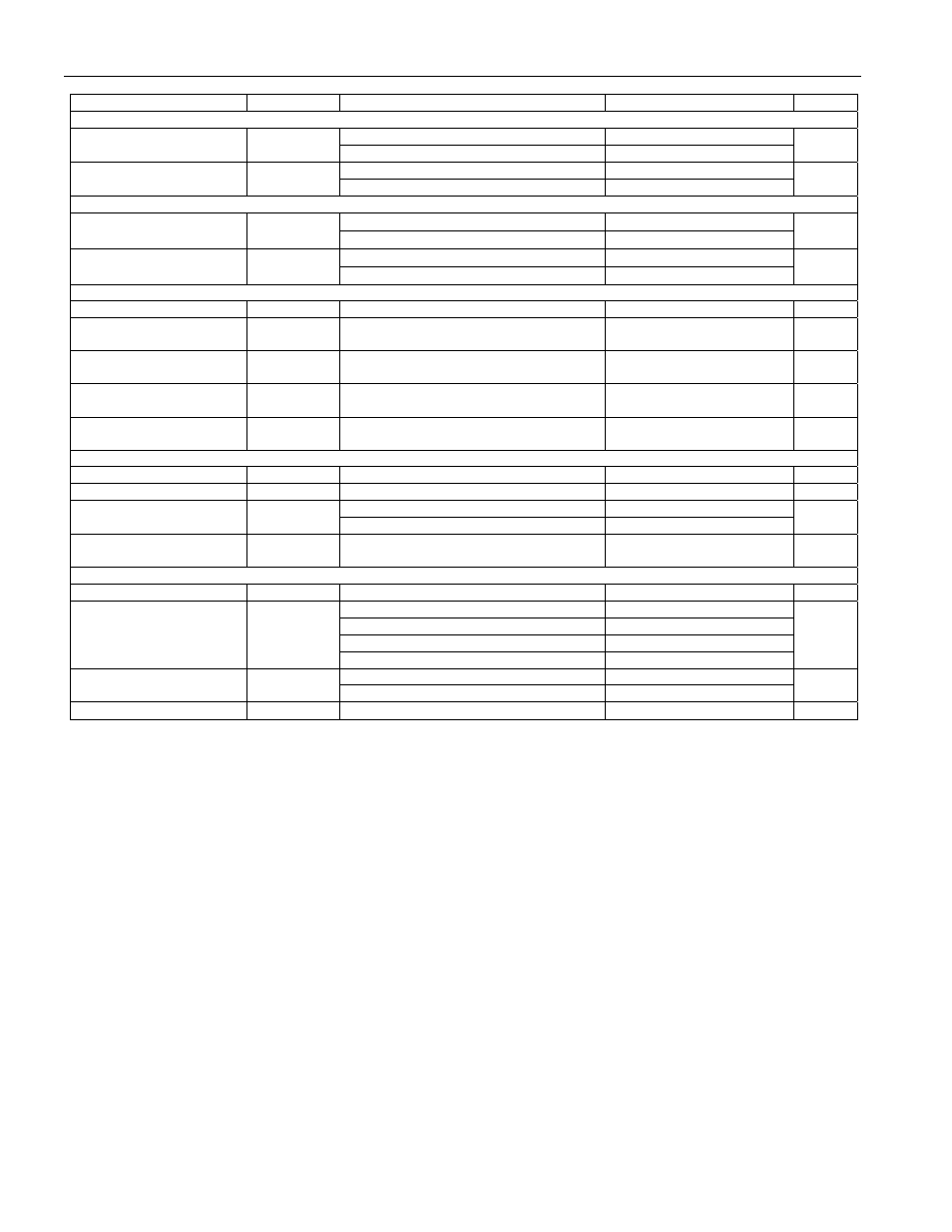
PARAMETER SYMBOL
CONDITIONS
MIN
TYP
MAX
UNITS
IO Pin, 1-Wire Write
Standard speed
60
120
Write-0 Low Time
(Notes 2, 17)
t
W0L
Overdrive speed
6
16
µs
Standard speed
5
15
Write-1 Low Time
(Notes 2, 17)
t
W1L
Overdrive speed
1
2
µs
IO Pin, 1-Wire Read
Standard speed
5
15 -
δ
Read Low Time
(Notes 2, 18)
t
RL
Overdrive speed
1
2 -
δ
µs
Standard speed
t
RL
+
δ
15
Read Sample Time
(Notes 2, 18)
t
MSR
Overdrive speed
t
RL
+
δ
2
µs
PIO Pins
Input Low Voltage
V
ILP
(Note 2)
0.3
V
Input High Voltage
(Note 2)
V
IHP
V
X
= max(V
PUP
, V
DD
) Vx-1.6
V
Input Load Current
(Note 19)
I
LP
Pin at GND
-1.1
µA
Output Low Voltage
(Note 11)
V
OLP
At 4mA
0.4
V
Chain-on Pullup
Impedance
R
CO
(Note
5)
20 40 60 k
Ω
EEPROM
Programming Current
I
PROG
(Notes 5, 20)
1.5
mA
Programming Time
t
PROG
(Note 21)
10
ms
At +25°C
200k
Write/Erase Cycles (En-
durance) (Notes 22, 23)
N
CY
-40°C to +85°C
50k
—
Data Retention
(Notes 24, 25)
t
DR
At +85°C (worst case)
10
years
Temperature Converter
Conversion Current
I
CONV
(Notes 5, 20)
1.5
mA
12-bit resolution (1/16°C)
750
11-bit resolution (1/8°C)
375
10-bit resolution (1/4°C)
187.5
Conversion Time
(Note 26)
t
CONV
9-bit resolution (1/2°C)
93.75
ms
-10°C to +85°C
-0.5
+0.5
Conversion Error
Δϑ
below -10°C (Note 5)
-0.5
+2.0
°C
Converter Drift
ϑ
D
(Note 27)
-0.2
+0.2
°C
Note 1:
Specifications at T
A
= -40°C are guaranteed by design only and not production-tested.
Note 2:
System requirement.
Note 3:
Maximum allowable pullup resistance is a function of the number of 1-Wire devices in the system and 1-Wire recovery times. The
specified value here applies to parasitically powered systems with only one device and with the minimum 1-Wire recovery
times. For more heavily loaded systems, local power or an active pullup such as that found in the DS2482-x00, DS2480B, or
DS2490 may be required. If longer t
REC
is used, higher R
PUP
values may be tolerable.
Note 4:
Value is 25pF max. with local power. Maximum value represents the internal parasite capacitance when V
PUP
is first applied. If
R
PUP
= 2.2k
Ω, 2.5µs after V
PUP
has been applied the parasite capacitance will not affect normal communications.
Note 5:
Guaranteed by design, characterization, and/or simulation only. Not production tested.
Note 6:
V
TL
, V
TH
, and V
HY
are a function of the internal supply voltage, which is itself a function V
DD
, V
PUP
, R
PUP
, 1-Wire timing, and
capacitive loading on IO. Lower V
DD
, V
PUP
, higher R
PUP
, shorter t
REC
, and heavier capacitive loading all lead to lower values of V
TL
,
V
TH
, and V
HY
.
Note 7:
Voltage below which, during a falling edge on IO, a logic '0' is detected.
Note 8:
The voltage on IO needs to be less than or equal to V
ILMAX
at all times the master drives the line to a logic '0'.
Note 9:
Voltage above which, during a rising edge on IO, a logic '1' is detected.
Note 10:
After V
TH
is crossed during a rising edge on IO, the voltage on IO has to drop by at least V
HY
to be detected as logic '0'.
Note 11:
The I-V characteristic is linear for voltages less than 1V.
Note 12:
Applies to a single parasitically powered DS28EA00 attached to a 1-Wire line. These values also apply to networks of multiple
DS28EA00 with local supply.
Note 13:
The earliest recognition of a negative edge is possible at t
REH
after V
TH
has been reached on the preceding rising edge.
Note 14:
Defines maximum possible bit rate. Equal to 1/(t
W0L(min)
+ t
REC(min)
).
Note 15:
Interval during the negative edge on IO at the beginning of a Presence-Detect pulse between the time at which the voltage is
80% of V
PUP
and the time at which the voltage is 20% of V
PUP
.
Note 16:
Interval after t
RSTL
during which a bus master is guaranteed to sample a logic '0' on IO if there is a DS28EA00 present. Minimum
limit is t
PDH(max)
+ t
FPD(max)
; maximum limit is t
PDH(min)
+ t
PDL(min)
.
Note 17:
ε in Figure 14 represents the time required for the pullup circuitry to pull the voltage on IO up from V
IL
to V
TH
. The actual maximum
duration for the master to pull the line low is t
W1Lmax
+ t
F
-
ε and t
W0Lmax
+ t
F
-
ε respectively.