Ds92001 pin description (soic and llp), Ac test circuits and timing diagrams – Rainbow Electronics DS92001 User Manual
Page 7

AC Test Circuits and Timing Diagrams
(Continued)
DS92001 Pin Description (SOIC and LLP)
Pin Name
Pin #
Input/Output
Description
GND
1
P
Ground
IN −
2
I
Inverting receiver B/LVDS input pin
IN+
3
I
Non-inverting receiver B/LVDS input pin
LOS
4
O
Loss of Signal output pin. LOS is asserted low while signal is invalid.
See Applications Information section.
V
CC
5
P
Power Supply, 3.3V
±
0.3V.
OUT+
6
O
Non-inverting driver BLVDS output pin
OUT -
7
O
Inverting driver BLVDS output pin
EN
8
I
Enable pin. When EN is LOW, the driver is disabled and the BLVDS
outputs are in TRI-STATE. When EN is HIGH, the driver is enabled.
LVCMOS/LVTTL levels.
GND
DAP
P
LLP Package Ground
20024742
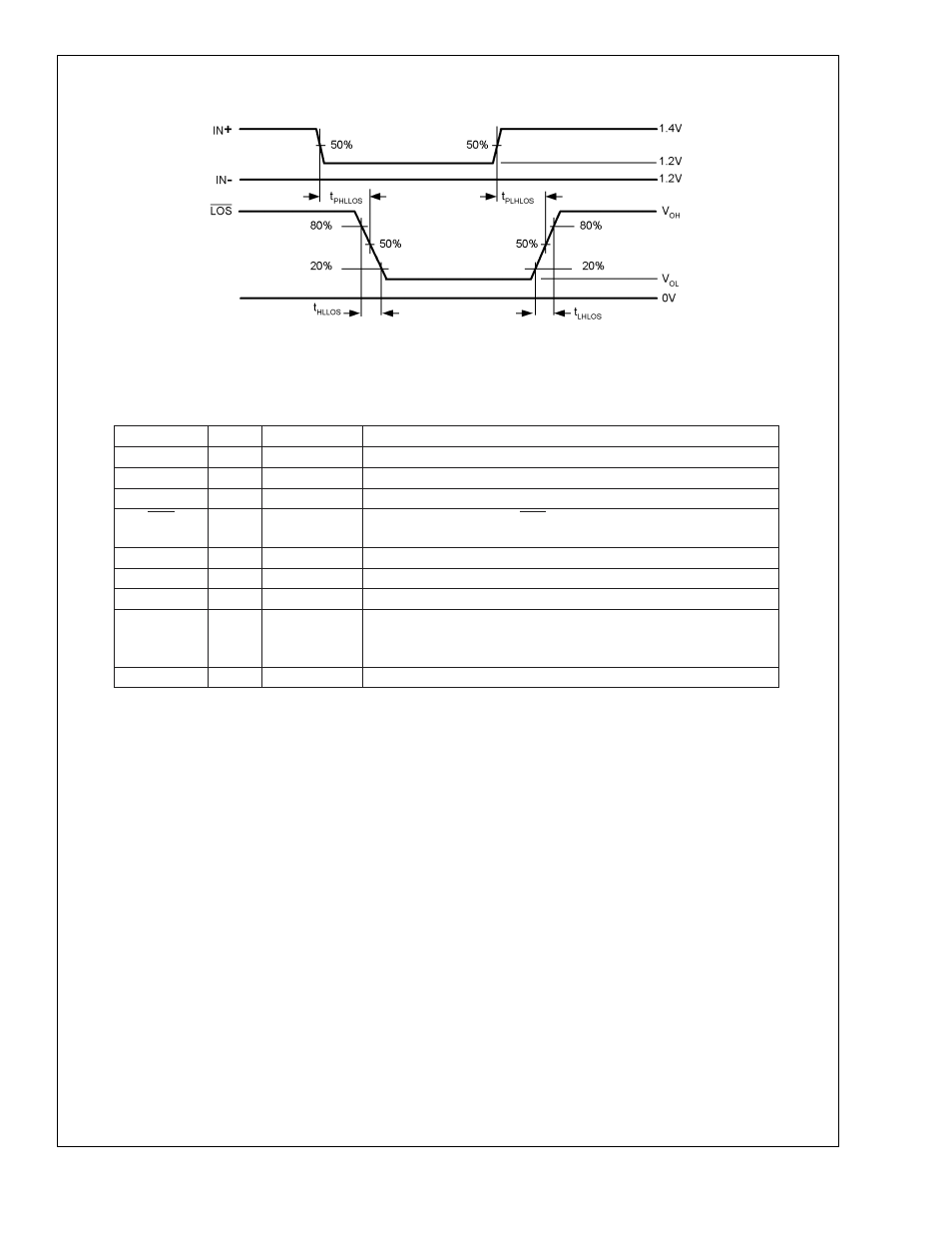
FIGURE 9. LOS Output Waveforms for Propagation Delay, and Rise/Fall Times
DS92001
www.national.com
7
See also other documents in the category Rainbow Electronics Control panel:
- MAX16840 (1 page)
- MAX9258 (54 pages)
- MAX66140 (21 pages)
- MAX9393 (14 pages)
- MAX66040 (25 pages)
- MAX6981 (1 page)
- MAX6965 (23 pages)
- MAX66100 (16 pages)
- MAX9135 (19 pages)
- MAX66020 (25 pages)
- MAX17127 (22 pages)
- MAX13175E (38 pages)
- MAX16820 (10 pages)
- MAX13237E (16 pages)
- MAX13483E (19 pages)
- MAX13362 (14 pages)
- MAX13486E (16 pages)
- MAX7311 (17 pages)
- MAX8759 (31 pages)
- SCAN92LV090 (13 pages)
- MAX6973 (23 pages)
- MAX13047E (14 pages)
- MAX16831 (20 pages)
- MAX14770E (15 pages)
- MAX11835 (1 page)
- MAX9621 (14 pages)
- MAX9217 (16 pages)
- MAX16841 (18 pages)
- MAX16834 (22 pages)
- MAX7315 (27 pages)
- MAX8645Y (15 pages)
- MAX6975 (23 pages)
- MAX6971 (12 pages)
- MAX3028 (21 pages)
- MAX9395 (13 pages)
- MAX7313 (27 pages)
- MAX6970 (1 page)
- MAX4821 (13 pages)
- MAX4895E (8 pages)
- MAX16823 (13 pages)
- MAX6963 (34 pages)
- MAX9216 (17 pages)
- MAX66000 (21 pages)
- MAX66120 (24 pages)
- MAX13223E (11 pages)
