Note 1), Note 5), High)(note 4) – Rainbow Electronics DS92001 User Manual
Page 4: Note 2), Note 4), Note 3), Note 10), Note 7), Note 8), Ac electrical characteristics
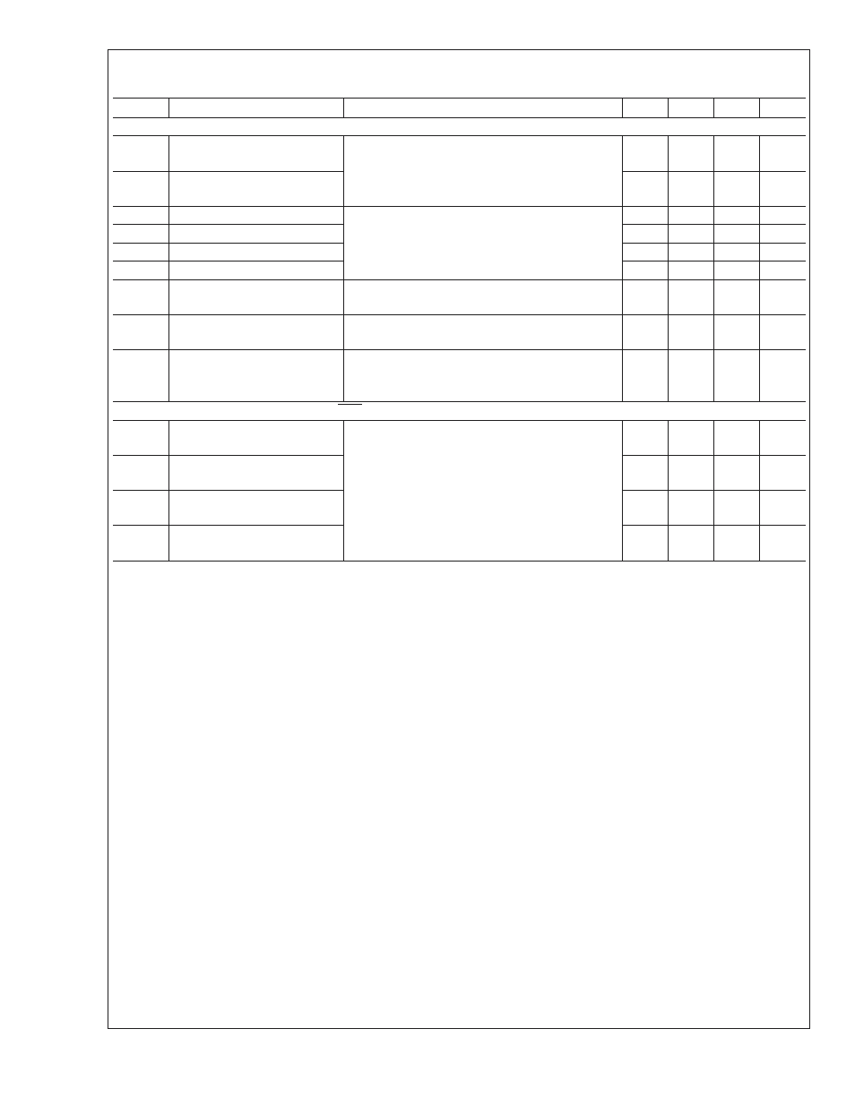
AC Electrical Characteristics
(Continued)
Over recommended operating supply and temperature ranges unless otherwise specified. (Note 3)
Symbol
Parameter
Conditions
Min
Typ
Max
Units
LVDS OUTPUT AC SPECIFICATIONS (OUT)
t
LHT
Rise Time (Notes 5, 10)
20% to 80% points
R
L
= 50
Ω or 27Ω, C
L
= 15pF
0.350
0.6
1.0
ns
t
HLT
Fall Time (Notes 5, 10)
80% to 20% points
0.350
0.6
1.0
ns
t
PHZ
Disable Time (Active High to Z) R
L
= 50
Ω, C
L
= 15pF
3
25
ns
t
PLZ
Disable Time (Active Low to Z)
3
25
ns
t
PZH
Enable Time (Z to Active High)
100
120
ns
t
PZL
Enable Time (Z to Active Low)
100
120
ns
t
DJ
LVDS Data Jitter, Deterministic
(Peak-to-Peak) (Note 9)
V
ID
= 300mV; PRBS = 2
23
− 1 data; V
CM
= 1.2V at
400Mbps (NRZ)
78
ps
t
RJ
LVDS Clock Jitter, Random
V
ID
= 300mV; V
CM
= 1.2V at 200MHz clock
36
ps
f
MAX
Maximum guaranteed
frequency
V
ID
= 200mV, V
CM
= 1.2V
200
300
MHz
LVCMOS/LVTTL AC SPECIFICATIONS (LOS)
t
PHLLOS
LVTTL Propagation Delay High
to Low (Note 5)
CL = 10pF, IN− = 1V, 1V
≤ IN+ ≤ 1.3V,
Freq. = 10MHz, 50% Duty Cycle
10
15
20
ns
t
PLHLOS
LVTTL Propagation Delay Low
to High (Note 5)
2
5
10
ns
t
LHLOS
Rise Time
20% to 80% (Note 5)
1
2
3
ns
t
HLLOS
Fall Time
80% to 20% (Note 5)
1
1.3
3
ns
Note 1: “Absolute Maximum Ratings” are those values beyond which the safety of the device cannot be guaranteed. They are not meant to imply that the device
should be operated at these limits. The table of “Electrical Characteristics” specifies conditions of device operation.
Note 2: Current into device pins is defined as positive. Current out of device pins is defined as negative. All voltages are referenced to ground except V
ID
, V
OD
, V
TH
,
V
TL
, and
∆V
OD
. V
OD
has a value and direction. Positive direction means OUT+ is a more positive voltage than OUT−.
Note 3: All typical are given for V
CC
= +3.3V and T
A
= +25˚C, unless otherwise stated.
Note 4: Output short circuit current (I
OS
) is specified as magnitude only, minus sign indicates direction only.
Note 5: The parameters are guaranteed by design. The limits are based on statistical analysis of the device performance over the PVT (process, voltage and
temperature) range.
Note 6: t
SKD1
, |t
PLHD
− t
PHLD
|, is the magnitude difference in differential propagation delay time between the positive going edge and the negative going edge of
the same channel (a measure of duty cycle).
Note 7: t
SKD3
, Part to Part Skew, is defined as the difference between the minimum and maximum specified differential propagation delays. This specification
applies to devices at the same V
CC
and within 5˚C of each other within the operating temperature range. This parameter guaranteed by design and characterization.
Note 8: t
SKD4
, Part to Part Skew, is the differential channel-to- channel skew of any event between devices. This specification applies to devices over recommended
operating temperature and voltage ranges, and across process distribution. t
SKD4
is defined as |Max − Min| differential propagation delay.
Note 9: The parameters are guaranteed by design. The limits are based on statistical analysis of the device performance over the PVT range with the following test
equipment setup: Agilent 86130A used as stimulus, 5 feet of RG142B cable with DUT test board and Agilent 86100A (digital scope mainframe) with Agilent 86122A
(20GHz scope module). Data input jitter pk to pk = 22 picoseconds; Clock input jitter = 24 picoseconds; t
DJ
measured 100 picoseconds, t
RJ
measured 60
picoseconds.
Note 10: Propagation delay, rise and fall times are guaranteed by design and characterization to 200MHz. Generator for these tests: 50MHz
≤ f ≤ 200MHz, Zo =
50
Ω, tr, tf ≤ 0.5ns. Generator used was HP8130A (300MHz capability).
Note 11: f
MAX
test: Generator (HP8133A or equivalent), Input duty cycle = 50%. Output criteria: VOD
≥ 200mV, Duty Cycle better than 45/55%. This specification
is guaranteed by design and characterization. A minimum is specified, which means that the device will operate to specified conditions from DC to the minimum
guaranteed AC frequency. The typical value is always greater than the minimum guarantee.
DS92001
www.national.com
4