Absolute maximum ratings, Parameter, Symbol – Rainbow Electronics DS18S20 User Manual
Page 19: Local power, Parasite power, Notes, 0v to 5.5v)
DS18S20
19 of 21
ABSOLUTE MAXIMUM RATINGS*
Voltage on any pin relative to ground
–0.5V to +6.0V
Operating temperature
–55
°
C to +125
°
C
Storage temperature
–55
°
C to +125
°
C
Soldering temperature
See J-STD-020A Specification
*These are stress ratings only and functional operation of the device at these or any other conditions
above those indicated in the operation sections of this specification is not implied. Exposure to absolute
maximum rating conditions for extended periods of time may affect reliability.
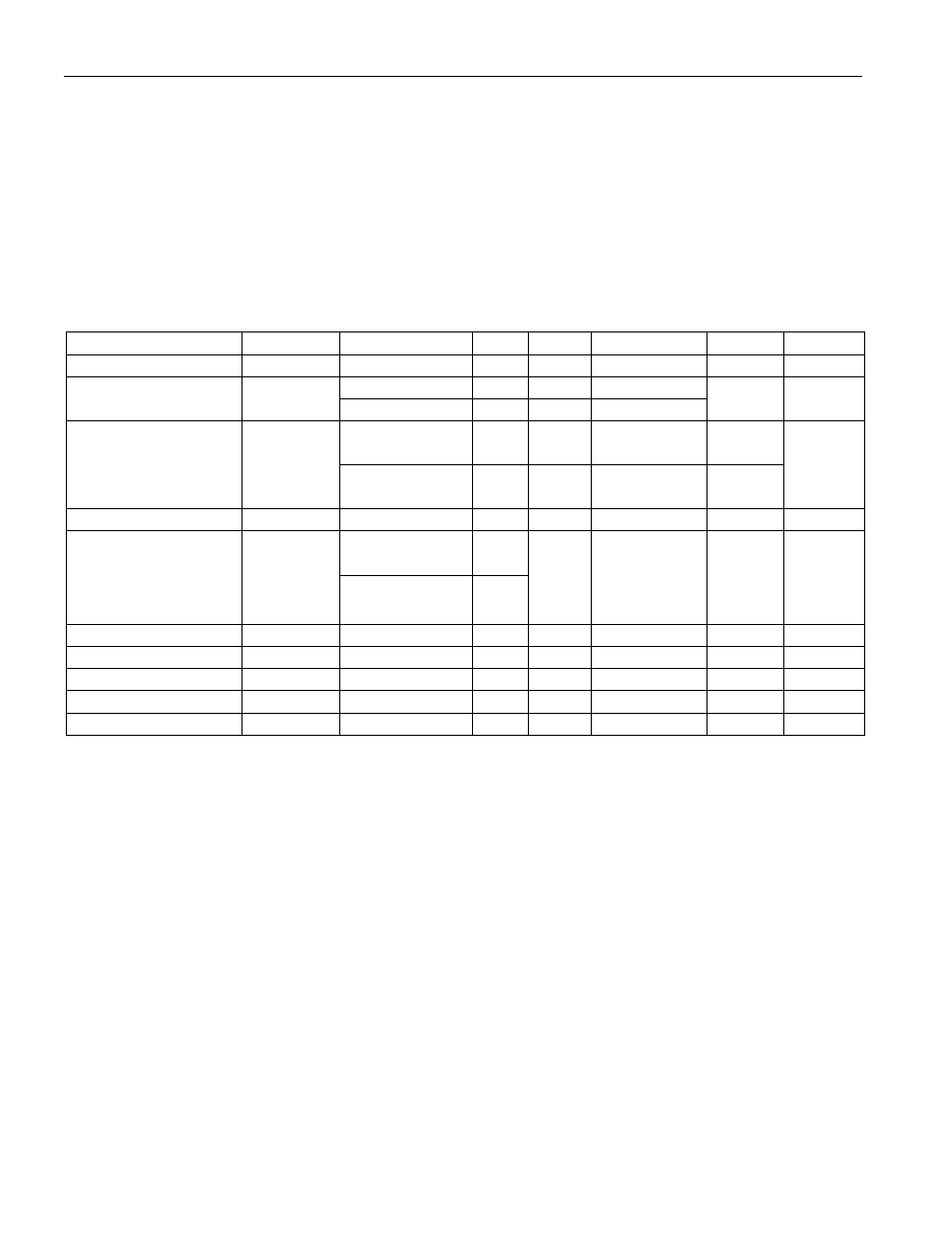
DC ELECTRICAL CHARACTERISTICS
(-55°C to +125°C; V
DD
=3.0V to 5.5V)
PARAMETER SYMBOL
CONDITION
MIN
TYP MAX
UNITS
NOTES
Supply Voltage
V
DD
Local
Power
+3.0
+5.5
V 1
Parasite Power
+3.0
+5.5
Pullup Supply
Voltage
V
PU
Local Power
+3.0
V
DD
V 1,2
-10°C to
+85°C
±0.5
°C
3
Thermometer Error
t
ERR
-55°C to
+125°C
±2
Input Logic Low
V
IL
-0.3
+0.8
V
1,4,5
Local Power
+2.2
Input Logic High
V
IH
Parasite Power
+3.0
The lower of
5.5
or
V
DD
+ 0.3
V 1,
6
Sink Current
I
L
V
I/O
=0.4V 4.0
mA 1
Standby Current
I
DDS
750 1000
nA 7,8
Active Current
I
DD
V
DD
=5V 1 1.5 mA 9
DQ Input Current
I
DQ
5
µA
10
Drift
±0.2
°C
11
NOTES:
1. All voltages are referenced to ground.
2. The Pullup Supply Voltage specification assumes that the pullup device is ideal, and therefore the
high level of the pullup is equal to V
PU
. In order to meet the V
IH
spec of the DS18S20, the actual
supply rail for the strong pullup transistor must include margin for the voltage drop across the
transistor when it is turned on; thus: V
PU_ACTUAL
= V
PU_IDEAL
+ V
TRANSISTOR
.
3. See typical performance curve in Figure 16
4. Logic low voltages are specified at a sink current of 4 mA.
5. To guarantee a presence pulse under low voltage parasite power conditions, V
ILMAX
may have to be
reduced to as low as 0.5V.
6. Logic high voltages are specified at a source current of 1 mA.
7. Standby current specified up to 70
°
C. Standby current typically is 3
µ
A at 125
°
C.
8. To
minimize
I
DDS
, DQ should be within the following ranges: GND
≤
DQ
≤
GND + 0.3V or V
DD
–
0.3V
≤
DQ
≤
V
DD
.
9. Active current refers to supply current during active temperature conversions or EEPROM writes.
10. DQ line is high (“hi-Z” state).
11. Drift data is based on a 1000 hour stress test at 125°C with V
DD
= 5.5V.