Absolute maximum ratings, Operating ratings (notes , ), Converter electrical characteristics – Rainbow Electronics ADC10D040 User Manual
Page 7: Operating ratings
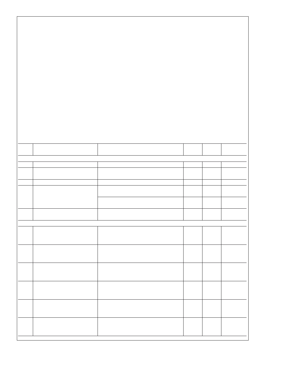
Absolute Maximum Ratings
(Notes 1,
If Military/Aerospace specified devices are required,
please contact the National Semiconductor Sales Office/
Distributors for availability and specifications.
Positive Supply Voltages
3.8V
Voltage on Any Pin
−0.3V to (V
A
or V
D
+0.3V)
Input Current at Any Pin (Note 3)
±
25 mA
Package Input Current (Note 3)
±
50 mA
Package Dissipation at T
A
= 25˚C
See (Note 4)
ESD Susceptibility (Note 5)
Human Body Model
2500V
Machine Model
250V
Soldering Temperature,
Infrared, 10 sec. (Note 6)
235˚C
Storage Temperature
−65˚C to +150˚C
Operating Ratings
(Notes 1, 2)
Operating Temperature Range
−40˚C
≤ T
A
≤ +85˚C
V
A
, V
D
Supply Voltage
+3.0V to +3.6V
V
DR
Supply Voltage
+1.5V to V
D
V
IN
Differential Voltage Range
GAIN = Low
±
V
REF
/2
GAIN = High
±
V
REF
V
CM
Input Common Mode Range
GAIN = Low
V
REF
/4 to (V
A
–V
REF
/4)
GAIN = High
V
REF
/2 to (V
A
–V
REF
/2)
V
REF
Voltage Range
0.6V to 1.8V
Digital Input Pins Voltage
Range
−0.3V to (V
A
+0.3V)
Converter Electrical Characteristics
The following specifications apply for V
A
= V
D
= +3.3 V
DC
, V
DR
= +2.5 V
DC
, V
REF
= 1.4 V
DC
, GAIN = OF = 0V, OS = 3.3V, V
IN
(a.c. coupled) = FSR = 1.4 V
P-P
, C
L
= 15 pF, f
CLK
= 40 MHz, 50% Duty Cycle, R
S
= 50
Ω, t
rc
= t
fc
<
4 ns, NOT offset cor-
rected. Boldface limits apply for T
A
= T
MIN
to T
MAX
: all other limits T
A
= 25˚C (Note 7).
Symbol
Parameter
Conditions
Typical
Limits
Units
(Limits)
STATIC CONVERTER CHARACTERISTICS
INL
Integral Non-Linearity
±
0.65
±
1.9
LSB (max)
DNL
Differential Non-Linearity
±
0.35
+1.2
−1.0
LSB (max)
LSB (min)
Resolution with No Missing Codes
10
Bits
V
OFF
Offset Error
Without Offset Correction
−3.3
+7
−12
LSB (max)
LSB (min)
With Offset Correction
+0.4
+1.5
−0.5
LSB (max)
LSB (min)
GE
Gain Error
−4
+5
−12
%FS (max)
%FS (min)
DYNAMIC CONVERTER CHARACTERISTICS
ENOB
Effective Number of Bits
f
IN
= 4.43 MHz, V
IN
= FSR −0.1 dB
9.5
Bits
f
IN
= 10.4 MHz, V
IN
= FSR −0.1 dB, T
A
= 25˚C
9.5
9.1
Bits (min)
f
IN
= 19.7 MHz, V
IN
= FSR −0.1 dB
9.4
Bits
SINAD
Signal-to-Noise Plus Distortion
Ratio
f
IN
= 4.43 MHz, V
IN
= FSR −0.1 dB
59
dB
f
IN
= 10.4 MHz, V
IN
= FSR −0.1 dB, T
A
= 25˚C
59
56.3
dB (min)
f
IN
= 19.7 MHz, V
IN
= FSR −0.1 dB
58
dB
SNR
Signal-to-Noise Ratio
f
IN
= 4.43 MHz, V
IN
= FSR −0.1 dB
60
dB
f
IN
= 10.4 MHz, V
IN
= FSR −0.1 dB, T
A
= 25˚C
60
57.3
dB (min)
f
IN
= 19.7 MHz, V
IN
= FSR −0.1 dB
59
dB
THD
Total Harmonic Distortion
f
IN
= 4.43 MHz, V
IN
= FSR −0.1 dB
−70
dB
f
IN
= 10.4 MHz, V
IN
= FSR −0.1 dB, T
A
= 25˚C
−69
−61
dB (min)
f
IN
= 19.7 MHz, V
IN
= FSR −0.1 dB
−67
dB
HS2
Second Harmonic
f
IN
= 4.43 MHz, V
IN
= FSR −0.1 dB
−86
dB
f
IN
= 10.4 MHz, V
IN
= FSR −0.1 dB
−83
dB
f
IN
= 19.7 MHz, V
IN
= FSR −0.1 dB
−81
dB
HS3
Third Harmonic
f
IN
= 4.43 MHz, V
IN
= FSR −0.1 dB
−73
dB
f
IN
= 10.4 MHz, V
IN
= FSR −0.1 dB
−73
dB
f
IN
= 19.7 MHz, V
IN
= FSR −0.1 dB
−72
dB
ADC10D040
www.national.com
7