Note 3), Note 4), Note 5) – Rainbow Electronics ADC10D040 User Manual
Page 10: Note 6), Note 7)
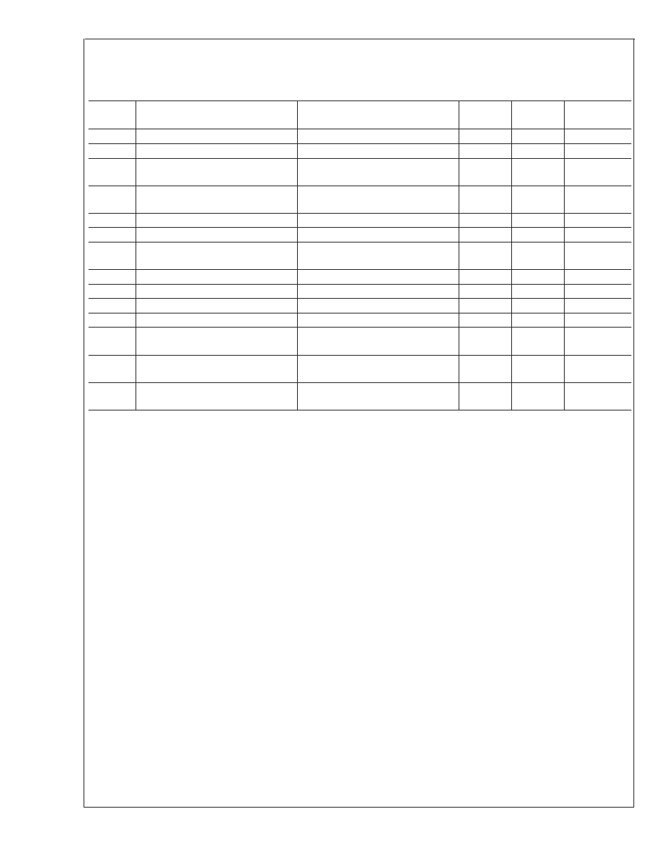
AC Electrical Characteristics
OS = High (Parallel Mode)
The following specifications apply for V
A
= V
D
= +3.3 V
DC
, V
DR
= +2.5V
DC
, V
REF
= 1.4 V
DC
, GAIN = OF = 0V, OS = +3.3V,
V
IN
(a.c. coupled) = FSR = 1.0 V
P-P
, C
L
= 15 pF, f
CLK
= 40 MHz, 50% Duty Cycle, R
S
= 50
Ω, t
rc
= t
fc
<
4 ns, NOT offset cor-
rected. Boldface limits apply for T
A
= T
MIN
to T
MAX
: all other limits T
A
= 25˚C (Note 7)
Symbol
Parameter
Conditions
Typical
Limits
Units
(Limits)
f
CLK1
Maximum Clock Frequency
45
40
MHz (min)
f
CLK2
Minimum Clock Frequency
20
MHz
Duty Cycle
50
45
55
% (min)
% (max)
Pipeline Delay (Latency)
2.5
Clock
Cycles
t
r
, t
f
Output Rise and Fall Times
9
ns
t
OC
OC Pulse Width
10
ns
t
OD
Output Delay from CLK Edge to
Data Valid
16
22
ns (max)
t
DIQ
I/Q Output Delay
13
ns
t
AD
Sampling (Aperture) Delay
2.2
ns
t
AJ
Aperture Jitter
<
10
ps (rms)
t
VALID
Data Valid Time
16
ns
Overrange Recovery Time
Differential V
IN
step from 1.5V to
0V
50
ns
t
WUPD
PD Low to 1/2 LSB Accurate
Conversion (Wake-Up Time)
<
1
ms
t
WUSB
STBY Low to 1/2 LSB Accurate
Conversion (Wake-Up Time)
800
ns
Note 1: Absolute Maximum Ratings indicate limits beyond which damage to the device may occur. Operating Ratings indicate conditions for which the device is
functional, but do not guarantee specific performance limits. For guaranteed specifications and test conditions, see the Electrical Characteristics. The guaranteed
specifications apply only for the test conditions listed. Some performance characteristics may degrade when the device is not operated under the listed test
conditions.
Note 2: All voltages are measured with respect to GND = AGND = DGND = 0V, unless otherwise specified.
Note 3: When the input voltage at any pin exceeds the power supplies (V
IN
<
GND or V
IN
>
V
A
or V
D
), the current at that pin should be limited to 25 mA. The 50 mA
maximum package input current rating limits the number of pins that can safely exceed the power supplies with an input current of 25 mA to two.
Note 4: The absolute maximum junction temperature (T
J
max) for this device is 150˚C. The maximum allowable power dissipation is dictated by T
J
max, the
junction-to-ambient thermal resistance (
θ
JA
), and the ambient temperature (T
A
), and can be calculated using the formula P
D
MAX = (T
J
max - T
A
)/
θ
JA
. In the 48-pin
TQFP,
θ
JA
is 76˚C/W, so P
D
MAX = 1,645 mW at 25˚C and 855 mW at the maximum operating ambient temperature of 85˚C. Note that the power dissipation of this
device under normal operation will typically be about 307 mW (267 mW quiescent power + 40 mW due to 1 LVTTL load on each digital output). The values for
maximum power dissipation listed above will be reached only when the ADC10D040 is operated in a severe fault condition (e.g. when input or output pins are driven
beyond the power supply voltages, or the power supply polarity is reversed). Obviously, such conditions should always be avoided.
Note 5: Human body model is 100 pF capacitor discharged through a 1.5 k
Ω resistor. Machine model is 220 pF discharged through 0Ω.
Note 6: See AN450, “Surface Mounting Methods and Their Effect on Product Reliability”, or the section entitled “Surface Mount” found in any post 1986 National
Semiconductor Linear Data Book, for other methods of soldering surface mount devices.
Note 7: The inputs are protected as shown below. Input voltage magnitude up to 300 mV beyond the supply rails will not damage this device. However, errors in
the A/D conversion can occur if the input goes beyond the limits given in these tables.
ADC10D040
www.national.com
10