Note 8), Note 9), Note 10) – Rainbow Electronics ADC10D040 User Manual
Page 11
AC Electrical Characteristics
OS = High (Parallel Mode)
(Continued)
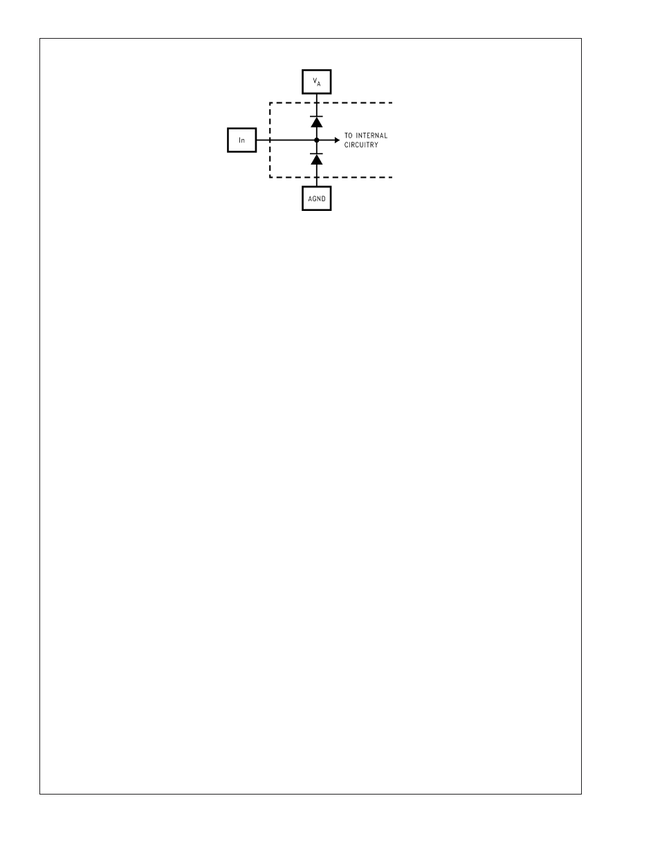
20029706
Note 8: Typical figures are at T
J
= 25˚C, and represent most likely parametric norms.
Note 9: Test limits are guaranteed to National’s AOQL (Average Outgoing Quality Level). Performance is guaranteed only at V
REF
= 1.4V and a clock duty cycle
of 50%. The limits for V
REF
and clock duty cycle specify the range over which reasonable performance is expected. Tests are performed and limits guaranteed with
clock low and high levels of 0.3V and V
D
−0.3V, respectively.
Note 10: I
DR
is the current consumed by the switching of the output drivers and is primarily determined by the load capacitance on the output pins, the supply
voltage, V
DR
, and the rate at which the outputs are switching (which is signal dependent). I
DR
= V
DR
(C
O
x f
O
+ C
1
x f
1
+ ... + C
9
x f
9
) where V
DR
is the output driver
power supply voltage, C
n
is the total capacitance on the output pin, and f
n
is the average frequency at which that pin is toggling.
ADC10D040
www.national.com
11