1 reference voltage, Applications information – Rainbow Electronics ADC10D040 User Manual
Page 24
Applications Information
(Continued)
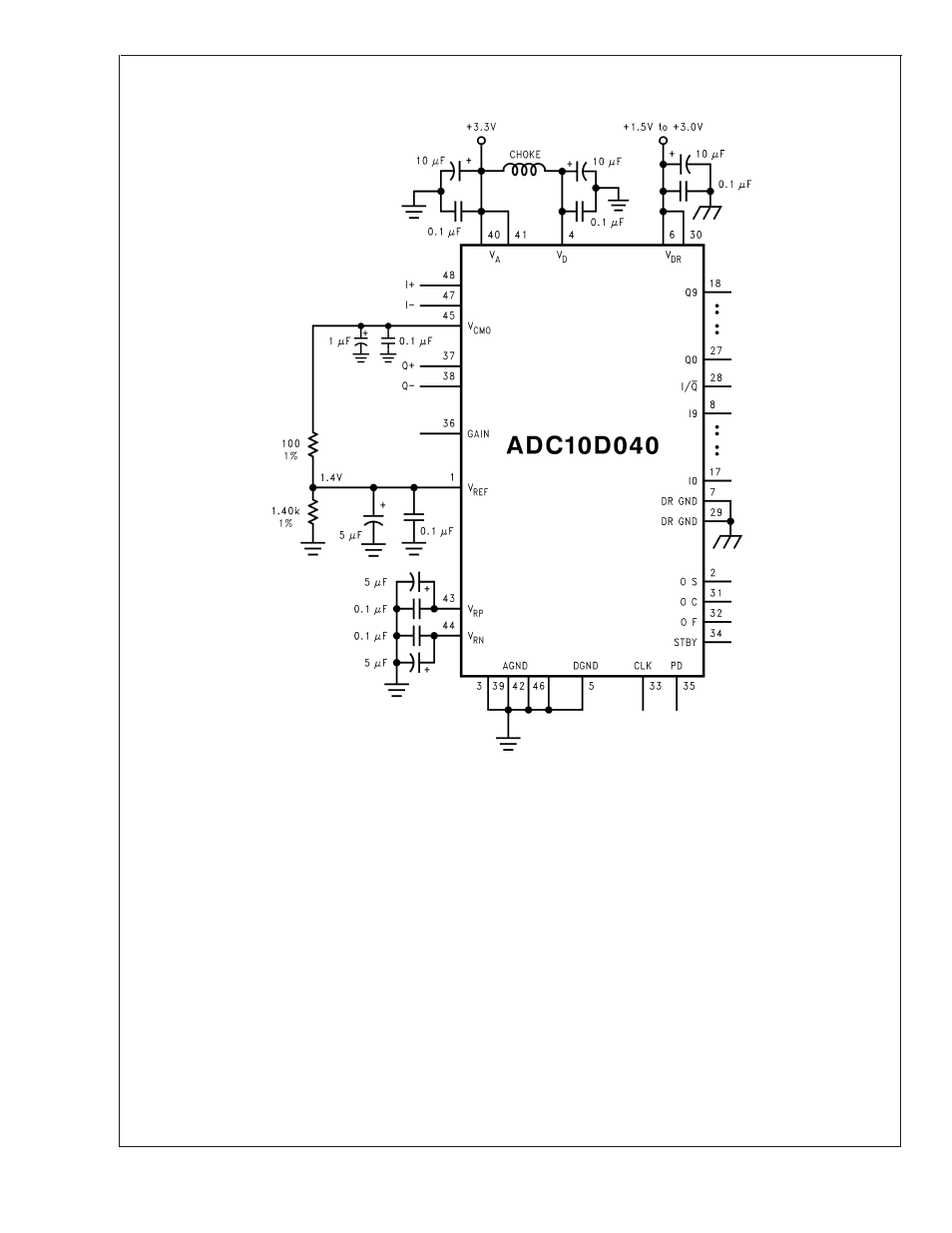
The V
CMO
output can be used as the ADC reference source
as long as care is taken to prevent excessive loading of this
pin. However, the V
CMO
output was not designed to be a
precision reference and has move variability than does a
precision reference. Refer to V
CMO
, Common Mode Voltage
Output, in the Electrical Characteristics table. Since the ref-
erence input of the ADC10D040 is buffered, there is virtually
no loading on the V
CMO
output by the V
REF
pin. While the
ADC10D040 will work with a 1.5V reference voltage, it is fully
specified for a 1.4V reference. To use the V
CMO
for a refer-
ence voltage at 1.4V, the 1.5V V
CMO
output needs to be
divided down. The divider resistor values need to be care-
fully chosen to prevent excessive V
CMO
loading. See Figure
7. While the average temperature coefficient of V
CMO
is 30
ppm/˚C, that temperature coefficient can be broken down to
a typical 70 ppm/˚C between −40˚C and +25˚C and a typical
−11 ppm/˚C between +25˚C and +85˚C.
2.1 Reference Voltage
The reference voltage should be within the range specified in
the Operating Ratings table (0.6V to 1.6V). A reference
voltage that is too low could result in a noise performance
that is less than desired because the quantization level falls
below other noise sources. On the other hand, a reference
voltage that is too high means that an input signal that
produces a full scale output uses such a large input range
that the input stage is less linear, resulting in a degradation
of distortion performance. Also, for large reference voltages,
the internal ladder buffer runs out of head-room, leading to a
reduction of gain in that buffer and causing gain error deg-
radation.
The Reference bypass pins V
RP
and V
RN
are output com-
pensated and should each be bypassed with a parallel com-
bination of a 5 µF (minimum) and 0.1 µF capacitors.
20029774
FIGURE 7. The V
CMO
output pin may be used as an internal reference source if its output is not loaded excessively.
ADC10D040
www.national.com
24