Functional description, Applications information, 0 the analog signal inputs – Rainbow Electronics ADC10D040 User Manual
Page 20: 0 reference inputs
Functional Description
Using a subranging architecture, the ADC10D040 achieves
9.4 effective bits over the entire Nyquist band at 40 MSPS
while consuming just 267 mW. The use of an internal
sample-and-hold amplifier (SHA) not only enables this sus-
tained dynamic performance, but also lowers the converter’s
input capacitance and reduces the number of external com-
ponents required.
Analog signals at the “I” and “Q” inputs that are within the
voltage range set by V
REF
and the GAIN pin are digitized to
ten bits at up to 45 MSPS. V
REF
has a range of 0.6V to 1.6V,
providing a differential peak-to-peak input range of 0.6 V
P-P
to 1.6 V
P-P
with the GAIN pin at a logic low, or a differential
input range of 1.2 V
P-P
to 3.2 V
P-P
with the GAIN pin at a
logic high. Differential input voltages less than −V
REF
/2 with
the GAIN pin low, or less than −V
REF
with the GAIN pin high
will cause the output word to indicate a negative full scale.
Differential input voltages greater than V
REF
/2 with the GAIN
pin low, or greater than V
REF
with the GAIN pin high, will
cause the output word to indicate a positive full scale.
Both “I” and “Q” channels are sampled simultaneously on the
falling edge of the clock input, while the timing of the data
output depends upon the mode of operation.
In the parallel mode, the “I” and “Q” output busses contain
the conversion result for their respective inputs. The “I” and
“Q” channel data are present and valid at the data output
pins t
OD
after the rising edge of the input clock. In the
multiplexed mode, “I” channel data is available at the digital
outputs t
OD
after the rise of the clock edge, while the “Q”
channel data is available at the I0 through I9 digital outputs
t
OD
after the fall of the clock. However, a delayed I/Q output
signal should be used to latch the output for best, most
consistent results.
Data latency in the parallel mode is 2.5 clock cycles. In the
multiplexed mode data latency is 2.5 clock cycles for the “I”
channel and 3.0 clock cycles for the “Q” channel. The
ADC10D040 will convert as long as the clock signal is
present and the PD and STBY pins are low.
Throughout this discussion,V
CM
refers to the Common Mode
input voltage of the ADC10D040 while V
CMO
refers to its
Common Mode output voltage.
Applications Information
1.0 THE ANALOG SIGNAL INPUTS
Each of the analog inputs of the ADC10D040 consists of a
switch (transmission gate) followed by a switched capacitor
amplifier. The capacitance seen at each input pin changes
with the clock level, appearing as about 2 pF when the clock
is low, and about 5 pF when the clock is high. This switching
action causes analog input current spikes that work with the
input source impedance to produce voltage spikes.
The LMH6702 and the CLC428 dual op amp have been
found to be a good amplifiers to drive the ADC10D040
because of their wide bandwidth and low distortion. They
also have good Differential Gain and Differential Phase per-
formance.
Care should be taken to avoid driving the input beyond the
supply rails, even momentarily, as during power-up.
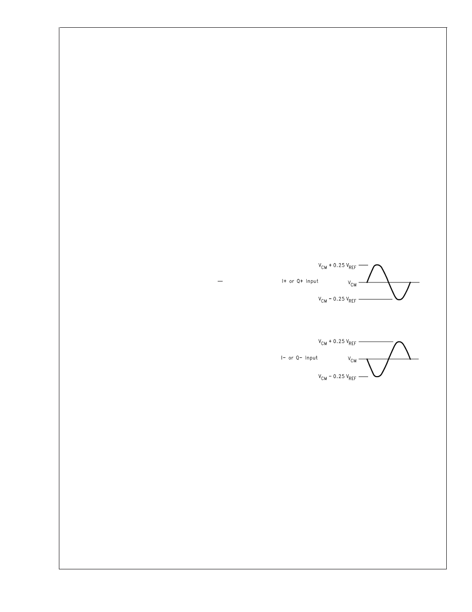
The ADC10D040 is designed for differential input signals for
best performance. With a 1.4V reference and the GAIN pin
at a logic low, differential input signals up to 1.4 V
P-P
are
digitized. See Figure 2. For differential signals, the input
common mode is expected to be about 1.5V, but the inputs
are not sensitive to the common-mode voltage and can be
anywhere within the supply rails (ground to V
A
) with little or
no performance degradation, as long as the signal swing at
the individual input pins is no more than 300 mV beyond the
supply rails.
Single-ended drive is not recommended as it can result in
degraded dynamic performance and faulty operation. If
single-ended input drive is absolutely required, it is recom-
mended that a sample rate above 30 MSPS be used. If the
desired sample rate is lower than this, operate the
ADC10D040 at a multiple of the desired rate and decimate
the output (use every "n"th sample).
For single-ended drive, operate the ADC10D040 with the
GAIN pin at a logic low, connect one pin of the input pair to
1.5V (V
CM
) through a resistor of 1k to 10 k Ohms, bypassing
this input pin to ground with a 1 uF capacitor. Drive the other
input pin of the input pair with 1.0 V
P-P
centered around 1.5V.
Because of the larger signal swing at one input for single-
ended operation, distortion performance will not be as good
as with a differential input signal. Alternatively, single-ended
to differential conversion with a transformer provides a quick,
easy solution for those applications not requiring response to
d.c. and low frequencies. See Figure 3. The 36
Ω resistors
and 56 pF capacitor values are chosen to provide a cutoff
frequency near the clock frequency to compensate for the
effects of input sampling. A lower time constant should be
used for undersampling applications.
2.0 REFERENCE INPUTS
The V
RP
and V
RN
pins should each be bypassed with a 5 µF
(or larger) tantalum or electrolytic capacitor and a 0.1 µF
ceramic capacitor. Use these pins only for bypassing. DO
NOT connect anything else to these pins.
Figure 4 shows a simple reference biasing scheme with
minimal components. While this circuit will suffice for many
applications, the value of the reference voltage will depend
upon the supply voltage.
The circuit of Figure 5 is an improvement over the circuit of
Figure 4 because the reference voltage is independent of
supply voltage. This reduces problems of reference voltage
20029769
FIGURE 2. The ADC10D040 is designed for use with
differential signals of 1.4 V
P-P
with a common mode
voltage of 1.5V. The signal swing should not cause any
pin to experience a swing more than 300 mV beyond
the supply rails.
ADC10D040
www.national.com
20