Rainbow Electronics BA6219BFP-Y User Manual
Page 5
402
Motor driver ICs
BA6219B / BA6219BFP-Y
F
Operation notes
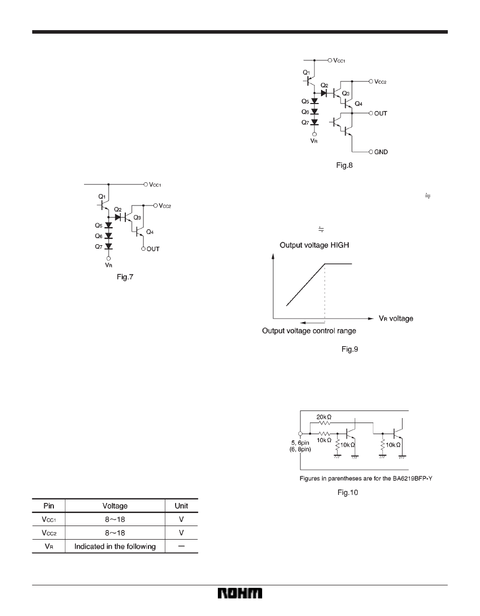
(1)
A schematic for the internal circuit associated with
the output voltage setting pin (Pin 4) is shown in Fig. 7.
The maximum output voltage (V
OMAX.
) is given by :
V
OMAX.
=V
CC1
*
V
SAT
(Q1)
*
V
BE
(Q2)
*
V
BE
(Q3)
*
V
BE
(Q4)
For the condition of V
R
being equal to or less than
V
OMAX.
, the relationship between the output voltage (V
O
)
and the pin 4 voltage is given by :
V
O
=V
R
)
{(V
BE
(Q5)
)
V
BE
(Q6)
)
V
BE
(Q7)
)
*
(V
BE
(Q2)
)
V
BE
(Q3)
)
V
BE
(Q4)
)}
Though
∆
V
BE
depends on the output power supply, V
O
is
nearly equal to V
R.
(2)
Thermal shutdown circuit
The thermal shutdown circuit turns off the driver output
if the chip temperature rises to about 180
_
. The shut-
down signal is not latched.
(3)
Power supply impedance
When the motor stops or starts, a rush current flows in the
VCC and GND lines. Depending on the way of connect-
ing a power supply decoupling capacitor (100
µ
F), the
control input voltage may become a negative value or the
supply voltage may drop to below the output voltage.
This can cause erratic operations due to parasitic effects.
Make sure that pin voltages will not exceed the supply
voltage by more than 0.3V or will not become less than
the GND pin voltage by more than 0.3V.
(4)
VCC1, VCC2, and VR are related to each other as
shown in the output circuit diagram of Fig. 8. Their values
should be kept within the following ranges.
Operating supply voltage ranges
(
1) When the output voltage control pin (pin 4) is used
V
R
< V
CC1
*
(V
SAT
(Q1)
)
V
BE
(Q5)
)
V
BE
(Q6)
)
V
BE
(Q7)
) V
CC1
*
2.5V
V
R
< V
CC2
*
{(V
SAT
(Q3)
*
V
BE
(Q3)
*
V
BE
(Q2)
)
)
(V
BE
(Q5)
)
V
BE
(Q6)
)
V
BE
(Q7)
)} V
CC2
*
1V
(
2) When the output voltage control pin (pin 4) is not
used, V
R
is either short-circuited to V
CC1
or left OPEN.
(5)
Input circuit