Rainbow Electronics MAX17117 User Manual
Page 14
Internal-Switch Boost Regulator with Integrated
7-Channel Scan Driver, Op Amp, and LDO
MAX17117
14 _____________________________________________________________________________________
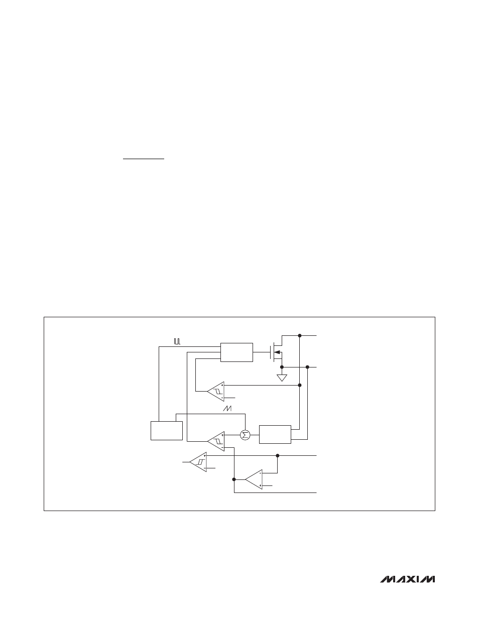
The regulator controls the output voltage and the power
delivered to the output by modulating the duty cycle (D)
of the internal power MOSFET in each switching cycle.
The duty cycle of the MOSFET is approximated by:
MAIN
IN
MAIN
V
V
D
V
−
≈
Figure 3 shows the step-up regulator block diagram.
An error amplifier compares the signal at FB to 1.24V
and changes the COMP output. The voltage at COMP
determines the current trip point each time the internal
MOSFET turns on. As the load varies, the error amplifier
sources or sinks current to the COMP output accord-
ingly to produce the inductor peak current necessary to
service the load. To maintain stability at high duty cycles,
a slope compensation signal is summed with the current-
sense signal.
On the rising edge of the internal clock, the controller sets
a flip-flop, turning on the n-channel MOSFET and apply-
ing the input voltage across the inductor. The current
through the inductor ramps up linearly, storing energy in
its magnetic field. Once the sum of the current-feedback
signal and the slope compensation exceed the COMP
voltage, the controller resets the flip-flop and turns off
the MOSFET. Since the inductor current is continuous,
a transverse potential develops across the inductor that
turns on the diode (D1). The voltage across the inductor
then becomes the difference between the output voltage
and the input voltage. This discharge condition forces
the current through the inductor to ramp back down,
transferring the energy stored in the magnetic field to the
output capacitor and the load. The MOSFET remains off
for the rest of the clock cycle.
Undervoltage Lockout (UVLO)
The UVLO circuit compares the input voltage at IN with
the UVLO threshold (2.0V typ) to ensure that the input
voltage is high enough for reliable operation. The 150mV
(typ) hysteresis prevents supply transients from caus-
ing a restart. Once the input voltage exceeds the UVLO
rising threshold, startup begins. When the input voltage
falls below the UVLO falling threshold, the controller
turns off the main step-up regulator.
Figure 3. Step-Up Regulator Block Diagram
FB
ERROR AMP
COMP
1.24V
PWM
COMPARATOR
CURRENT
SENSE
1.2MHz
OSCILLATOR
SLOPE COMP
ILIM
COMPARATOR
LOGIC AND
DRIVER
I
LIMIT
LX
PGND
CLOCK
1.10V
TO FAULT LOGIC
FAULT
COMPARATOR