Connection diagrams, Pin descriptions – Rainbow Electronics ADC12662 User Manual
Page 9
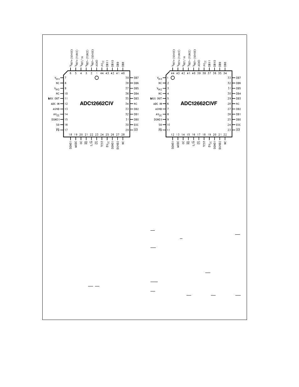
Connection Diagrams
TL H 11876 – 15
Top View
TL H 11876 – 29
Top View
Pin Descriptions
AV
CC
These are the two positive analog supply
inputs They should always be connected
to the same voltage source
but are
brought out separately to allow for sepa-
rate bypass capacitors Each supply pin
should be bypassed to AGND with a
0 1 mF ceramic capacitor in parallel with a
10 mF tantalum capacitor
DV
CC
This is the positive digital supply input It
should always be connected to the same
voltage as the analog supply AV
CC
It
should be bypassed to DGND2 with a
0 1 mF ceramic capacitor in parallel with a
10 mF tantalum capacitor
AGND
These are the power supply ground pins
DGND1
There are separate analog and digital
DGND2
ground pins for separate bypassing of the
analog and digital supplies The ground
pins should be connected to a stable
noise-free system ground
All of the
ground pins should be returned to the
same potential
AGND is the analog
ground for the converter DGND1 is the
ground pin for the digital control lines
DGND2 is the ground return for the output
databus See Section 6 0 LAYOUT AND
GROUNDING for more information
DB0 – DB11
These are the TRI-STATE output pins en-
abled by RD CS and OE
V
IN1
V
IN2
These are the analog input pins to the mul-
tiplexer For accurate conversions no in-
put pin (even one that is not selected)
should be driven more than 50 mV below
ground or 50 mV above V
CC
MUX OUT
This is the output of the on-board analog
input multiplexer
ADC IN
This is the direct input to the 12-bit sam-
pling A D converter For accurate conver-
sions this pin should not be driven more
than 50 mV below ground or 50 mV above
V
CC
S0
This pin selects the analog input that will
be connected to the ADC12662 during the
conversion The input is selected based on
the state of S0 when EOC makes its high-
to-low transition Low selects V
IN1
high
selects V
IN2
MODE
This pin should be tied to DGND1
CS
This is the active low Chip Select control
input When low this pin enables the RD
S H and OE inputs This pin can be tied
low
INT
This is the active low Interrupt output
When using the Interrupt Interface Mode
(Figure 1)
this output goes low when a
conversion has been completed and indi-
cates that the conversion result is avail-
able in the output latches This output is
always high when RD is held low
(Figure
2)
EOC
This is the End-of-Conversion control out-
put This output is low during a conversion
RD
This is the active low Read control input
When RD is low (and CS is low) the INT
output is reset and (if OE is high) data ap-
pears on the data bus This pin can be tied
low
9