Applications information – Rainbow Electronics ADC12662 User Manual
Page 13

Applications Information
(Continued)
2 0 THE ANALOG INPUT
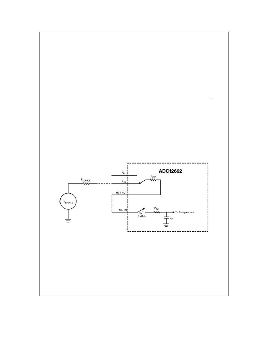
The analog input of the ADC12662 can be modeled as two
small resistances in series with the capacitance of the input
hold capacitor (C
IN
) as shown in
Figure 7
The S H switch
is closed during the Sample period and open during Hold
The source has to charge C
IN
to the input voltage within the
sample period Note that the source impedance of the input
voltage (R
SOURCE
) has a direct effect on the time it takes to
charge C
IN
If R
SOURCE
is too large the voltage across C
IN
will not settle to within 0 5 LSBs of V
SOURCE
before the
conversion begins and the conversion results will be incor-
rect From a dynamic performance viewpoint the combina-
tion of R
SOURCE
R
MUX
R
SW
and C
IN
form a low pass
filter Minimizing R
SOURCE
will increase the frequency re-
sponse of the input stage of the converter
Typical values for the components shown in
Figure 7
are
R
MUX
e
100X R
SW
e
100X and C
IN
e
25 pF The set-
tling time to n bits is
t
SETTLE
e
(R
SOURCE
a
R
MUX
a
R
SW
)
C
IN
n
ln (2)
The bandwidth of the input circuit is
f
b
3dB
e
1 (2
3 14
(R
SOURCE
a
R
MUX
a
R
SW
)
C
IN
)
The ADC12662 is operated in a pipelined sequence with
one hold capacitor acquiring the next sample while a con-
version is being performed on the voltage stored on the
other hold capacitor This gives the source over t
CONV
sec-
onds to charge the hold capacitor to its final value At
1 5 MHz the settling time must be less than 667 ns Using
the settling time equation and component values given
the maximum source impedance that will allow the input to
settle to
LSB (n e 13) at full speed is E2 8 kX To
ensure
LSB settling over temperature and device-to-de-
vice variation R
SOURCE
should be a maximum of 500X
when the converter is operated at full speed
If the signal source has a high output impedance its output
should be buffered with an operational amplifier capable of
driving a switched 25 pF 100X load Any ringing or instabili-
ties at the op amp’s output during the sampling period can
result in conversion errors The LM6361 high speed op amp
is a good choice for this application due to its speed and its
ability to drive large capacitive loads
Figure 8
shows the
LM6361 driving the ADC IN input of an ADC12662 The 100
pF capacitor at the input of the converter absorbs some of
the high frequency transients generated by the S H switch-
ing reducing the op amp transient response requirements
The 100 pF capacitor should only be used with high speed
op amps that are unconditionally stable driving capacitive
loads
Another benefit of using a high speed buffer is improved
THD performance when using the multiplexer of the
ADC12662 The MUX on-resistance is somewhat non-linear
over input voltage causing the RC time constant formed by
C
IN
R
MUX
and R
SW
to vary depending on the input voltage
This results in increasing THD with increasing frequency
Inserting the buffer between the MUX OUT and the ADC IN
terminals as shown in
Figure 8
will eliminate the loading on
R
MUX
significantly reducing the THD of the multiplexed sys-
tem
TL H 11876 – 19
FIGURE 7 Simplified ADC12662 Input Stage
13
