Absolute maximum ratings, Operating ratings, Converter characteristics – Rainbow Electronics ADC12662 User Manual
Page 2
Absolute Maximum Ratings
(Notes 1 2)
If Military Aerospace specified devices are required
please contact the National Semiconductor Sales
Office Distributors for availability and specifications
Supply Voltage (V
CC
e
DV
CC
e
AV
CC
)
b
0 3V to a6V
Voltage at Any Input or Output
b
0 3V to V
CC
a
0 3V
Input Current at Any Pin (Note 3)
25 mA
Package Input Current (Note 3)
50 mA
Power Dissipation (Note 4)
ADC12662CIV
875 mW
ESD Susceptibility (Note 5)
2000V
Soldering Information (Note 6)
V Package Infrared 15 seconds
a
300 C
VF Package
Vapor Phase (60 seconds)
215 C
Infrared (15 seconds)
220 C
Storage Temperature Range
b
65 C to a150 C
Maximum Junction Temperature (T
JMAX
)
150 C
Operating Ratings
(Notes 1 2)
Temperature Range
T
MIN
s
T
A
s
T
MAX
ADC12662CIV ADC12662CIVF
b
40 C
s
T
A
s
a
85 C
Supply Voltage Range (DV
CC
e
AV
CC
)
4 75V to 5 25V
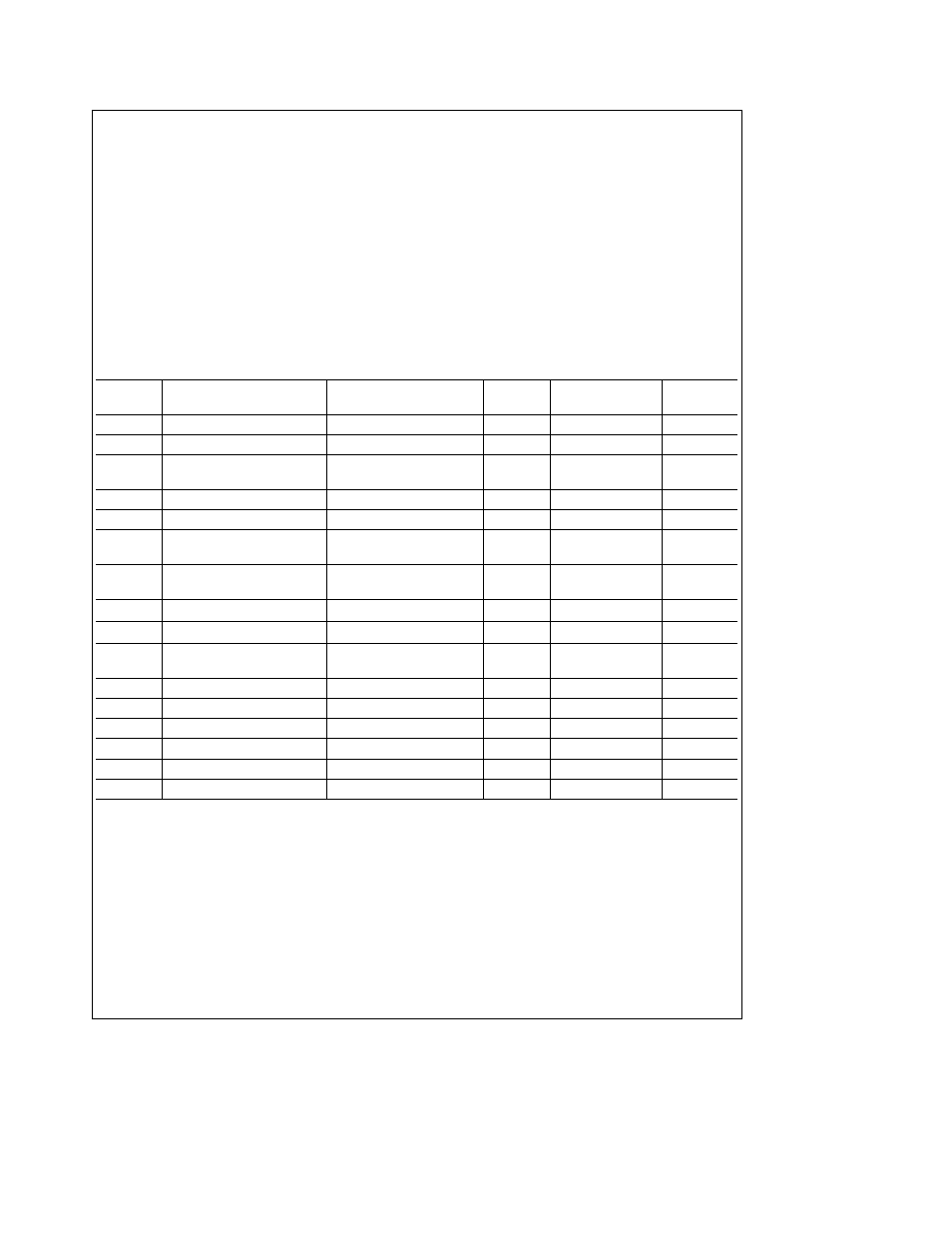
Converter Characteristics
The following specifications apply for DV
CC
e
AV
CC
e
a
5V V
REF
a
(SENSE)
e
a
4 096V V
REF
b
(SENSE)
e
AGND and f
s
e
1 5 MHz unless otherwise specified Boldface limits apply for T
A
e
T
J
from T
MIN
to T
MAX
all other limits T
A
e
T
J
e a
25 C
Symbol
Parameter
Conditions
Typ
Limit
Units
(Note 7)
(Note 8)
(Limit)
Resolution
12
Bits
Differential Linearity Error
T
MIN
to T
MAX
g
0 4
g
0 95
LSB (max)
Integral Linearity Error
T
MIN
to T
MAX
g
0 4
g
1 5
LSB (max)
(Note 9)
Offset Error
T
MIN
to T
MAX
g
0 3
g
2 0
LSB (max)
Full-Scale Error
T
MIN
to T
MAX
g
0 3
g
1 5
LSB (max)
Power Supply Sensitivity
DV
CC
e
AV
CC
e
5V
g
5%
g
0 75
LSB (max)
(Note 15)
R
REF
Reference Resistance
750
500
X
(min)
1000
X
(max)
V
REF(
a
)
V
REF
a
(SENSE)
Input Voltage
AV
CC
V (max)
V
REF(
b
)
V
REF
b
(SENSE)
Input Voltage
AGND
V (min)
V
IN
Input Voltage Range
To V
IN1
V
IN2
or ADC IN
AV
CC
a
0 05V
V (max)
AGND b 0 05V
V (min)
ADC IN Input Leakage
AGND to AV
CC
b
0 3V
0 1
3
m
A (max)
C
ADC
ADC IN Input Capacitance
25
pF
MUX On-Channel Leakage
AGND to AV
CC
b
0 3V
0 1
3
m
A (max)
MUX Off-Channel Leakage
AGND to AV
CC
b
0 3V
0 1
3
m
A (max)
C
MUX
Multiplexer Input Cap
7
pF
MUX Off Isolation
f
IN
e
100 kHz
92
dB
2