Functional description, Applications information – Rainbow Electronics ADC12662 User Manual
Page 12
Functional Description
(Continued)
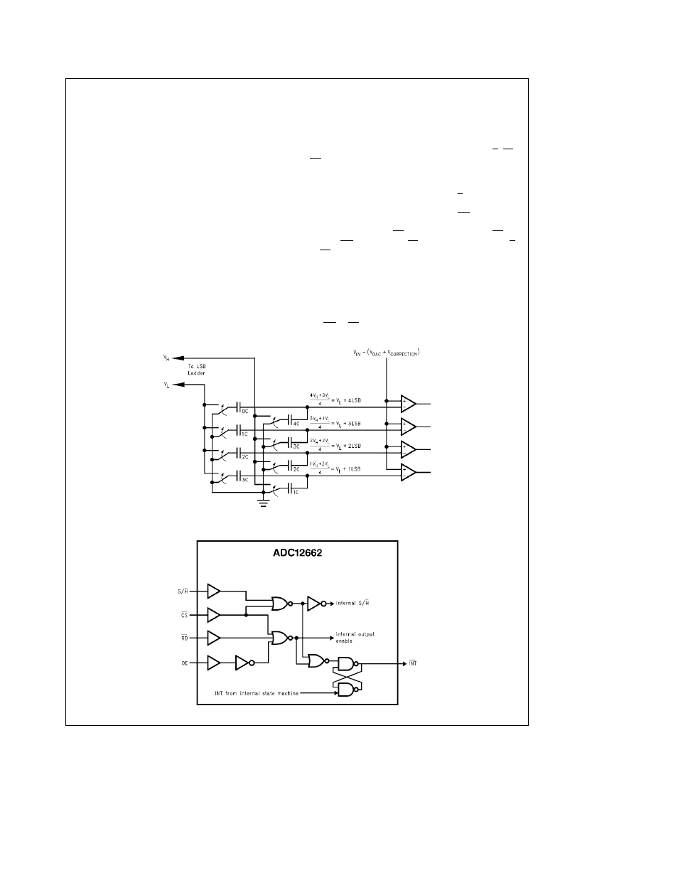
The result of this second conversion is accurate to 10 bits
and describes the input remainder as a voltage between two
tap points (V
H
and V
L
) on the LSB ladder To resolve the
last two bits the voltage across the ladder resistor (between
V
H
and V
L
) is divided up into 4 equal parts by the capacitive
voltage divider shown in
Figure 5
The divider also creates
6 LSBs below V
L
and 6 LSBs above V
H
to provide overlap
used by the digital error correction SW1 is moved to posi-
tion 3 and the remainder is compared with these 16 new
voltages The output is combined with the results of the
Voltage Estimator first flash and second flash to yield the
final 12-bit result
By using the same sixteen comparators for all three flash
conversions the number of comparators needed by the
multi-step converter is significantly reduced when compared
to standard multi-step techniques
Applications Information
1 0 MODES OF OPERATION
The ADC12662 has two interface modes An interrupt read
mode and a high speed mode
Figures 1
and
2
show the
timing diagrams for these interfaces
In order to clearly show the relationship between S H CS
RD and OE the control logic decoding section of the
ADC12662 is shown in
Figure 6
Interrupt Interface
As shown in
Figure 1
the falling edge of S H holds the input
voltage and initiates a conversion At the end of the conver-
sion the EOC output goes high and the INT output goes
low indicating that the conversion results are latched and
may be read by pulling RD low The falling edge of RD re-
sets the INT line Note that CS must be low to enable S H
or RD
High Speed Interface
The Interrupt interface works well at lower speeds but few
microprocessors could keep up with the 1 ms interrupts that
would be generated if the ADC12662 was running at full
speed The most efficient interface is shown in
Figure 2
Here the output data is always present on the databus and
the INT to RD delay is eliminated
TL H 11876 – 17
FIGURE 5 The Capacitive Voltage Divider
TL H 11876 – 18
FIGURE 6 ADC Control Logic
12