Applications information – Rainbow Electronics ADC12662 User Manual
Page 18

Applications Information
(Continued)
edge) of an MM74HC4538 one-shot The 1k resistor and
12 pF capacitor set the pulse length to approximately 100
ns The S H pulse stream for the converter appears on the
Q output of the HC4538 This is the S H clock generator
used on the ADC12062EVAL evaluation board For lower
power a CMOS inverter-based crystal oscillator can be
used in place of the DIP crystal oscillator See Application
Note AN-340 in the National Semiconductor CMOS Logic
Databook for more information on CMOS crystal oscillators
8 0 COMMON APPLICATION PITFALLS
Driving inputs (analog or digital) outside power supply
rails
The Absolute Maximum Ratings state that all inputs
must be between GND b 300 mV and V
CC
a
300 mV This
rule is most often broken when the power supply to the
converter is turned off but other devices connected to it (op
amps microprocessors) still have power Note that if there
is no power to the converter DGND e AGND e DV
CC
e
AV
CC
e
0V so all inputs should be within
g
300 mV of
AGND and DGND
Driving a high capacitance digital data bus
The more
capacitance the data bus has to charge for each conver-
sion the more instantaneous digital current required from
DV
CC
and DGND These large current spikes can couple
back to the analog section decreasing the SNR of the con-
verter While adequate supply bypassing and separate ana-
log and digital ground planes will reduce this problem buff-
ering the digital data outputs (with a pair of MM74HC541s
for example) may be necessary if the converter must drive a
heavily loaded databus
9 0 APPLICATIONS
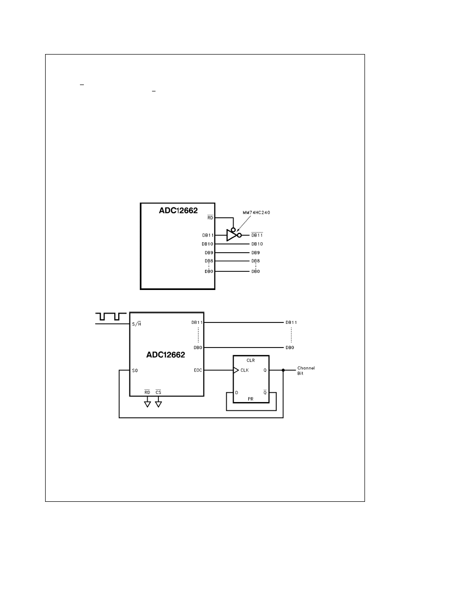
2’s Complement Output
TL H 11876 – 26
Ping-Ponging between V
IN1
and V
IN2
TL H 11876 – 27
18
