Pin descriptions, Functional description – Rainbow Electronics ADC12662 User Manual
Page 10
Pin Descriptions
(Continued)
OE
This is the active high Output Enable con-
trol input This pin can be thought of as an
inverted version of the RD input (see
Fig-
ure 6
) Data output pins DB0 – DB11 are
TRI-STATE when OE is low Data appears
on DB0 – DB11 only when OE is high and
CS and RD are both low This pin can be
tied high
S H
This is the Sample Hold control input The
analog input signal is held and a new con-
version is initiated by the falling edge of
this control input (when CS is low)
PD
This is the Power Down control input This
pin should be held high for normal opera-
tion When this pin is pulled low the device
goes into a low power standby mode
V
REF
a
(FORCE)
These are the positive and negative volt-
V
REF
b
(FORCE)
age reference force inputs respectively
See Section 4 REFERENCE INPUTS for
more information
V
REF
a
(SENSE)
These are the positive and negative volt-
V
REF
b
(SENSE)
age reference sense pins
respectively
See Section 4 REFERENCE INPUTS for
more information
V
REF
16
This pin should be bypassed to AGND with
a 0 1 mF ceramic capacitor
TEST
This pin should be tied to DV
CC
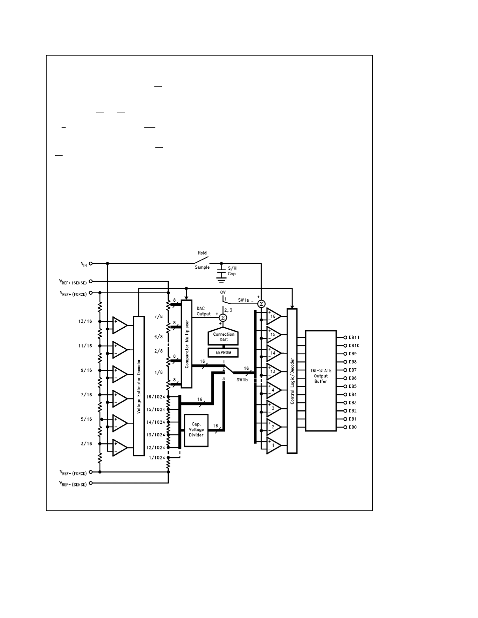
Functional Description
The ADC12662 performs a 12-bit analog-to-digital conver-
sion using a 3 step flash technique The first flash deter-
mines the six most significant bits the second flash gener-
ates four more bits and the final flash resolves the two least
significant bits
Figure 4
shows the major functional blocks
of the converter It consists of a 2
-bit Voltage Estimator a
resistor ladder with two different resolution voltage spans a
sample hoId capacitor a 4-bit flash converter with front end
multiplexer a digitally corrected DAC and a capacitive volt-
age divider To pipeline the converter there are two sam-
ple hold capacitors and 4-bit flash sections which allows
the converter to acquire the next input sample while con-
verting the previous one Only one of the flash converter
pairs is shown in
Figure 4
to reduce complexity
TL H 11876 – 16
FIGURE 4 Functional Block Diagram
10