Rainbow Electronics MAX66120 User Manual
Page 4
MAX66120
ISO 15693-Compliant 1Kb Memory Fob
4
_______________________________________________________________________________________
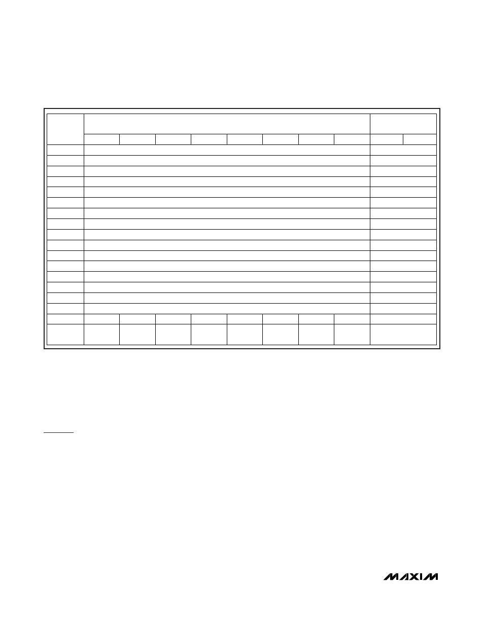
DATA BYTE NUMBER
(SEQUENCE LEFT TO RIGHT AS WRITTEN TO OR READ FROM DEVICE)
INTEGRITY BYTES
BLOCK
NUMBER
0
1
2
3
4
5
6
7
LSB
MSB
00h
Page 0 User EEPROM R/(W)
Write-Cycle Counter
01h
Page 0 User EEPROM R/(W)
Write-Cycle Counter
02h
Page 0 User EEPROM R/(W)
Write-Cycle Counter
03h
Page 0 User EEPROM R/(W)
Write-Cycle Counter
04h
Page 1 User EEPROM R/(W)
Write-Cycle Counter
05h
Page 1 User EEPROM R/(W)
Write-Cycle Counter
06h
Page 1 User EEPROM R/(W)
Write-Cycle Counter
07h
Page 1 User EEPROM R/(W)
Write-Cycle Counter
08h
Page 2 User EEPROM R/(W)
Write-Cycle Counter
09h
Page 2 User EEPROM R/(W)
Write-Cycle Counter
0Ah
Page 2 User EEPROM R/(W)
Write-Cycle Counter
0Bh
Page 2 User EEPROM R/(W)
Write-Cycle Counter
0Ch
Page 3 User EEPROM R/(W)
Write-Cycle Counter
0Dh
Page 3 User EEPROM R/(W)
Write-Cycle Counter
0Eh
Page 3 User EEPROM R/(W)
Write-Cycle Counter
0Fh
Page 3 User EEPROM R/(W)
Write-Cycle Counter
10h U1 U2 U3 U4 AFI
DSFID
U5 U6
Write-Cycle
Counter
11h BP1 BP2 BP3 BP4
U-Lock
AFI-Lock
DSFID-
Lock
S-Lock Write-Cycle
Counter
Figure 4. Memory Map
bit locations 49 to 56 identifies the chip manufacturer,
according to ISO/IEC 7816-6/AM1. This code is 2Bh
for Maxim. The code in the upper 8 bits is E0h. The
UID is read accessible through the Inventory and Get
System Information commands.
Detailed Memory Description
The memory of the MAX66120 is organized as 18
blocks of 8 bytes each. Figure 4 shows the memory
map. The first 16 blocks (block numbers 00h to 0Fh in
hexadecimal counting) are the user EEPROM, the area
for application-specific data. Four adjacent blocks are
also referred to as a page. Blocks 00h to 03h are
page 0, blocks 04h to 07h are page 1, blocks 08h to
0Bh are page 2, and blocks 0Ch to 0Fh are page 3.
Block 10h provides storage for user-programmable
parameters that are defined by the ISO 15693 stan-
dard. These are AFI and DSFID. The remaining bytes
(U1 to U6) are not defined by the communication stan-
dard; the application software can use them, e.g., for
proprietary markings. Block 11h contains control bytes
that determine the operation of the individual pages
(EPROM-emulation mode or write protection of individ-
ual blocks), or to write protect U1 to U4, the AFI, and
the DSFID byte. The S-Lock byte, if programmed to a
suitable code, only protects itself from future changes.
The self-protection feature can be used to permanently
mark the fob as being “special,” as defined by the
application. Table 1 illustrates the relationship between
the controlling register in block 11h and the memory
area affected. Tables 2 and 3 specify the code assign-
ments to achieve the protection.
Besides the storage for 8 data bytes, each memory
block has 2 integrity bytes, which are not memory
mapped. The integrity bytes function as a MAX66120-
maintained, 16-bit write-cycle counter. Having reached
its maximum value of 65,535, the write-cycle counter
stops incrementing, but does not prevent additional
write cycles to the memory block. The integrity bytes
can be read through the Custom Read Block command.