Electrical characteristics (continued) – Rainbow Electronics MAX5858 User Manual
Page 6

MAX5858
Dual, 10-Bit, 300Msps, Current-Output DAC with
4x/2x/1x Interpolation Filters
6
_______________________________________________________________________________________
ELECTRICAL CHARACTERISTICS (continued)
(AV
DD
= DV
DD
= CV
DD
= 3V, AGND = DGND = CGND = 0, f
DAC
= 165Msps, no interpolation, external reference, V
REF
= 1.2V,
I
FS
= 20mA, output amplitude = 0dB FS, differential output, T
A
= T
MIN
to T
MAX
, unless otherwise noted. T
A
> +25°C guaranteed by
production test. T
A
< +25°C guaranteed by design and characterization. Typical values are at T
A
= +25°C.)
PARAMETER
SYMBOL
CONDITIONS
MIN
TYP
MAX
UNITS
No interpolation
34
2x interpolation
75
f
DAC
= 60Msps
4x interpolation
72
No interpolation
54
61
2x interpolation
146
f
DAC
= 165Msps
4x interpolation
140
2x interpolation
172
186
Digital Supply Current (Note 4)
I
DVDD
f
DAC
= 200Msps
4x interpolation
165
178
mA
Clock Power-Supply Voltage
CV
DD
2.7
3.3
V
f
DAC
= 60Msps
25
f
DAC
= 165Msps
69
80
Clock Supply Current (Note 4)
I
CVDD
f
DAC
= 200Msps, 2x interpolation or 4x
interpolation
80
94
mA
Standby Current
I
STANDBY
(Note 5)
4.4
4.8
mA
Power-Down Current
I
PD
(Note 5)
1
µA
No interpolation
312
2x interpolation
435
f
DAC
= 60Msps
4x interpolation
426
No interpolation
504
570
2x interpolation
780
f
DAC
= 165Msps
4x interpolation
762
2x interpolation
891
Total Power Dissipation
P
TOT
f
DAC
= 200Msps
4x interpolation
870
mW
Note 1: Including the internal reference voltage tolerance.
Note 2: Measured single ended with 50
Ω load and complementary output connected to ground.
Note 3: Guaranteed by design, not production tested.
Note 4: f
OUT
= 5MHz.
Note 5: All digital inputs at 0 or DV
DD
. Clock signal disabled.
TO OUTPUT
PIN
5pF
0.5mA
0.5mA
1.6V
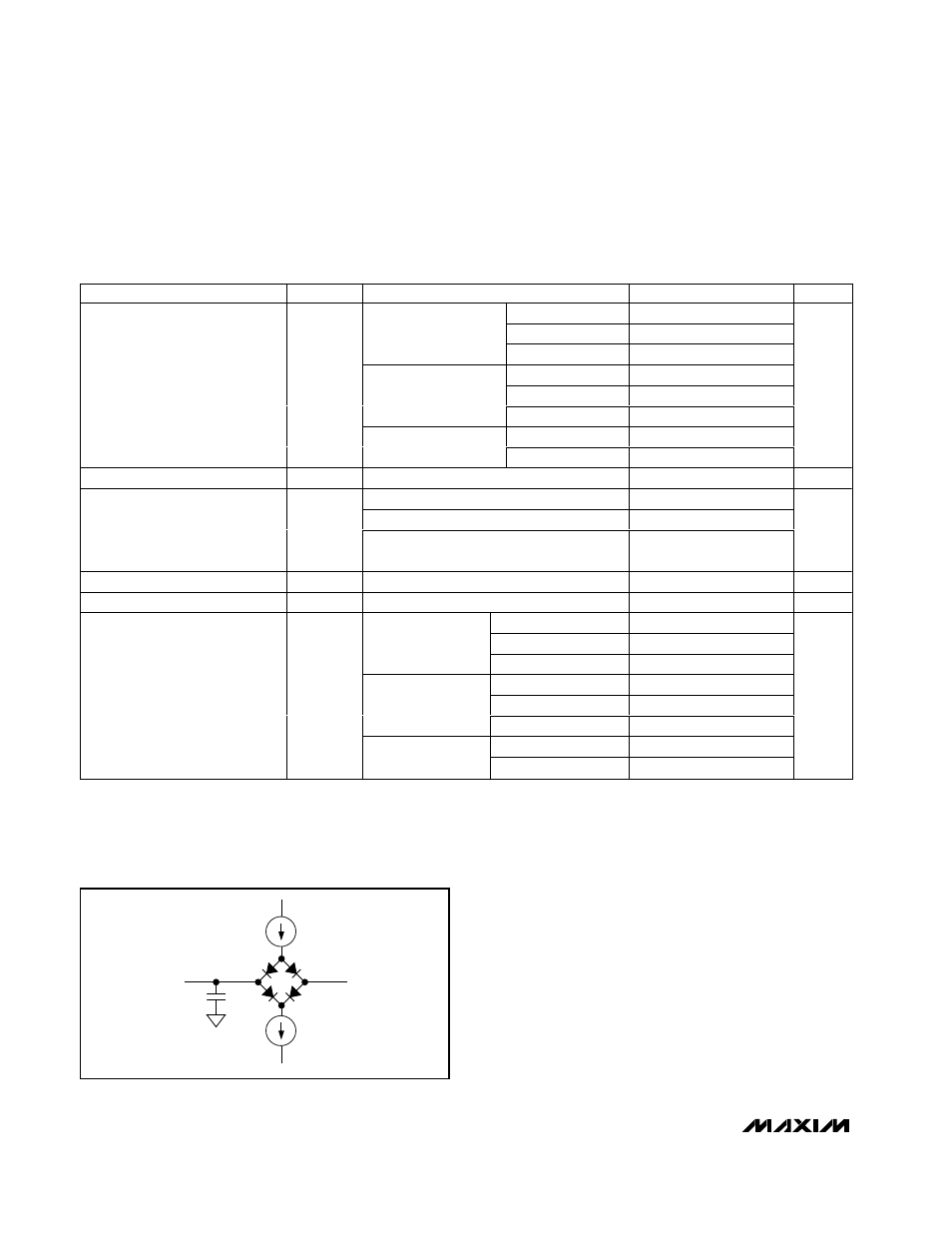
Figure 1. Load Test Circuit for CLK Outputs
