Rainbow Electronics MAX5858 User Manual
Page 2
MAX5858
Dual, 10-Bit, 300Msps, Current-Output DAC with
4x/2x/1x Interpolation Filters
2
_______________________________________________________________________________________
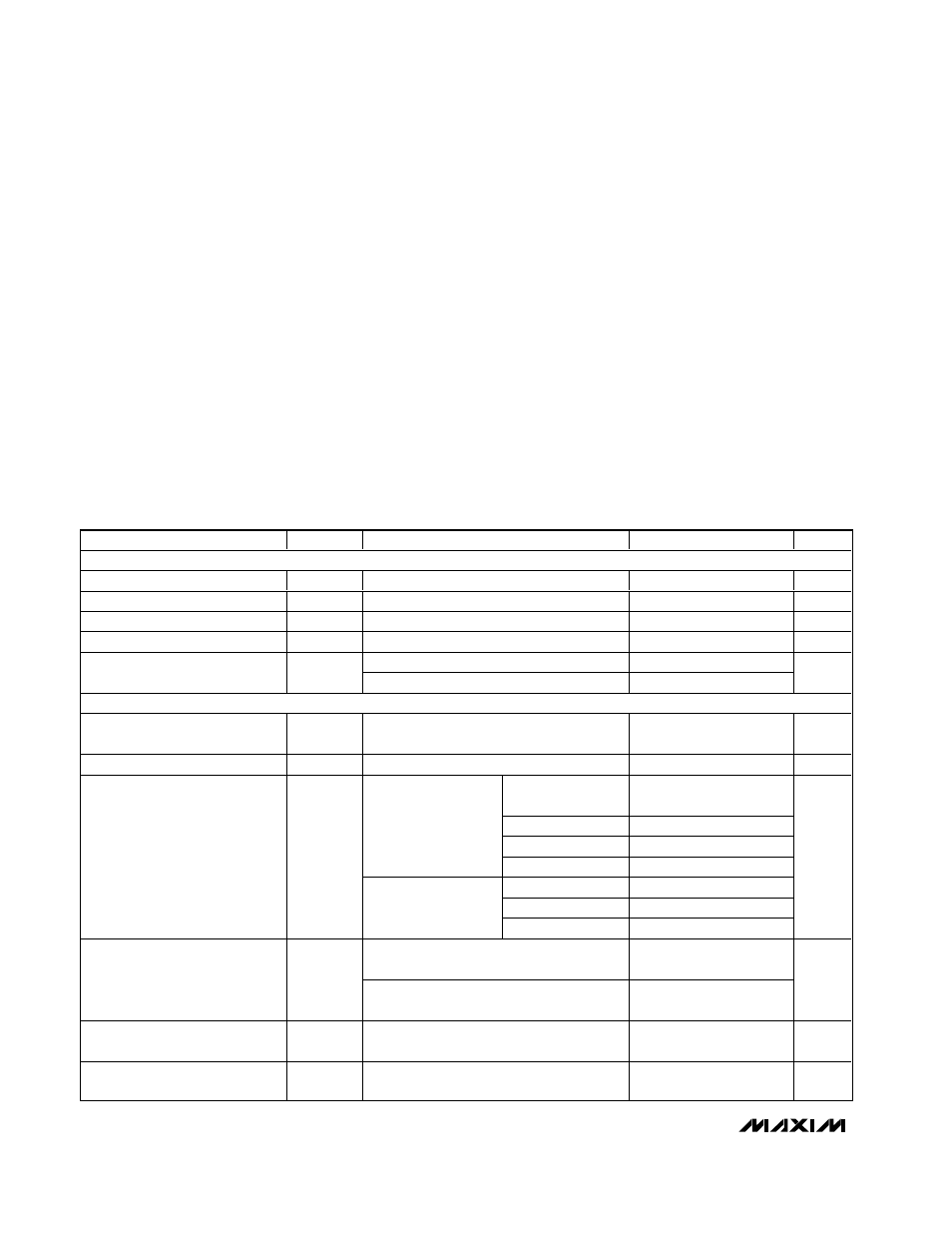
ABSOLUTE MAXIMUM RATINGS
ELECTRICAL CHARACTERISTICS
(AV
DD
= DV
DD
= CV
DD
= 3V, AGND = DGND = CGND = 0, f
DAC
= 165Msps, no interpolation, external reference, V
REF
= 1.2V,
I
FS
= 20mA, output amplitude = 0dB FS, differential output, T
A
= T
MIN
to T
MAX
, unless otherwise noted. T
A
> +25°C guaranteed by
production test. T
A
< +25°C guaranteed by design and characterization. Typical values are at T
A
= +25°C.)
Stresses beyond those listed under “Absolute Maximum Ratings” may cause permanent damage to the device. These are stress ratings only, and functional
operation of the device at these or any other conditions beyond those indicated in the operational sections of the specifications is not implied. Exposure to
absolute maximum rating conditions for extended periods may affect device reliability.
AV
DD
, DV
DD
, CV
DD
to AGND, DGND, CGND .........-0.3V to +4V
DA9–DA0, DB9–DB0, CW, REN to AGND,
DGND, CGND .......................................................-0.3V to +4V
IDE to AGND, DGND, CGND...................-0.3V to (DV
DD
+ 0.3V)
CLKXN, CLKXP to CGND.........................................-0.3V to +4V
OUTP_, OUTN_ to AGND.......................-1.25V to (AV
DD
+ 0.3V)
CLK to DGND ..........................................-0.3V to (DV
DD
+ 0.3V)
REFR, REFO to AGND .............................-0.3V to (AV
DD
+ 0.3V)
AGND to DGND, DGND to CGND,
AGND to CGND..................................................-0.3V to +0.3V
Maximum Current into Any Pin
(excluding power supplies) ............................................±50mA
Continuous Power Dissipation (T
A
= +70°C)
48-Pin TQFP-EP (derate 36.2mW/°C above +70°C) ....2.898W
Operating Temperature Range ...........................-40°C to +85°C
Storage Temperature Range .............................-65°C to +150°C
Junction Temperature ......................................................+150°C
Lead Temperature (soldering, 10s) .................................+300°C
PARAMETER
SYMBOL
CONDITIONS
MIN
TYP
MAX
UNITS
STATIC PERFORMANCE
Resolution
10
Bits
Integral Nonlinearity
INL
R
L
= 0
-1.25
±0.5
+1.25
LSB
Differential Nonlinearity
DNL
Guaranteed monotonic, R
L
= 0
-0.75
±0.25
+0.75
LSB
Offset Error
V
OS
-0.5
±0.1
+0.5
LSB
Internal reference (Note 1)
-9
±1.5
+10
Gain Error (See Gain Error
Parameter Definitions Section)
GE
External reference
-5
±1.5
+7
%
DYNAMIC PERFORMANCE
Maximum Output DAC Update
Rate
f
DAC
300
Msps
Glitch Impulse
5
pV-s
f
OUT
= 5MHz,
T
A
≥ +25°C
69
76
f
OUT
= 20MHz
75
f
OUT
= 40MHz
65
f
DAC
= 165Msps
f
OUT
= 60MHz
63
f
OUT
= 5MHz
76
f
OUT
= 40MHz
78
Spurious-Free Dynamic Range to
Input Update Rate Nyquist
SFDR
f
DAC
= 300Msps,
2x interpolation
f
OUT
= 60MHz
70
dBc
f
DAC
= 200Msps, 2x interpolation;
f
OUT
= 40MHz, span = 20MHz
85
Spurious-Free Dynamic Range
Within a Window
SFDR
f
DAC
= 165Msps, f
OUT
= 5MHz,
span = 4MHz
78
85
dBc
Multitone Power Ratio, 8 Tones,
300kHz Spacing
MTPR
f
DAC
= 165Msps, f
OUT
= 20MHz
76
dBc
Adjacent Channel Leakage Ratio
with UMTS
ACLR
f
DAC
=122.88Msps, f
OUT
= 30.72MHz
63
dB