Rainbow Electronics MAX5858 User Manual
Page 17

MAX5858
Dual, 10-Bit, 300Msps, Current-Output DAC with
4x/2x/1x Interpolation Filters
______________________________________________________________________________________
17
I
FS
C
COMP
*
REFR
I
REF
REFO
MAX4040
1.24V
BANDGAP
REFERENCE
CURRENT-
SOURCE ARRAY
*COMPENSATION CAPACITOR (C
COMP
≈ 100nF).
OPTIONAL EXTERNAL BUFFER
FOR HEAVIER LOADS
REN
MAX5858
I
REF
=
V
REF
R
SET
R
SET
AGND
AGND
AGND
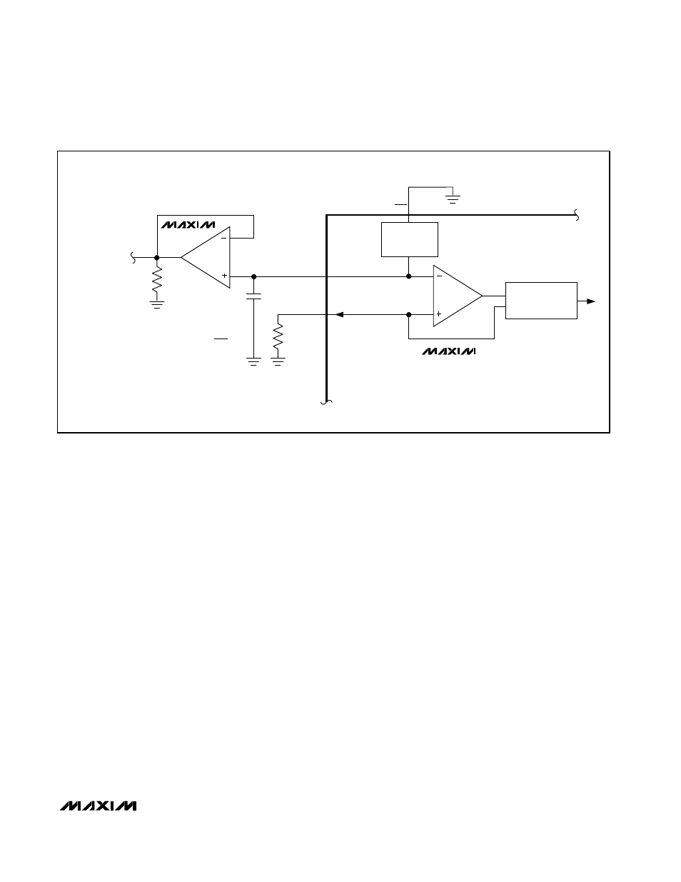
Figure 4. Setting IFS with the Internal 1.24V Reference and the Control Amplifier
Clocking Modes
Apply an external clock to CLKXP and CLKXN at the
desired DAC update rate and allowable input ampli-
tude. CLK is an output and provides the signal neces-
sary to synchronize the input data. CLKXP and CLKXN
accept a frequency range of 0 to 300MHz (see Table
5). Maintain a low capacitive load at the CLK output
(not higher than 10pF for f
CLK
of 165MHz).
Internal Reference and Control Amplifier
The MAX5858 provides an integrated 50ppm/°C, 1.24V,
low-noise bandgap reference that can be disabled and
overridden with an external reference voltage. REFO
serves either as an external reference input or an inte-
grated reference output. If REN is connected to AGND,
the internal reference is selected and REFO provides a
1.24V (50µA) output. Buffer REFO with an external
amplifier, when driving a heavy load.
The MAX5858 also employs a control amplifier
designed to simultaneously regulate the full-scale out-
put current (I
FS
) for both outputs of the devices.
Calculate the output current as:
I
FS
= 32
✕
I
REF
where I
REF
is the reference output current (I
REF
=
V
REFO
/R
SET
) and I
FS
is the full-scale output current.
R
SET
is the reference resistor that determines the ampli-
fier output current of the MAX5858 (Figure 4). This cur-
rent is mirrored into the current-source array where I
FS
is equally distributed between matched current seg-
ments and summed to valid output current readings for
the DACs.
External Reference
To disable the internal reference of the MAX5858, con-
nect REN to AV
DD
. Apply a temperature-stable, external
reference to drive the REFO to set the full-scale output
(Figure 5). For improved accuracy and drift performance,
choose a fixed output voltage reference such as the
1.24V, 25ppm/°C MAX6520 bandgap reference.
Detailed Timing
The MAX5858 accepts an input data rate up to 165MHz
or the DAC conversion rate of 300MHz. The input latch-
es on the rising edge of the clock, whereas the output
latches on the following rising edge.
Figure 6 depicts the write cycle of the DACs in 4x inter-
polation mode. In this timing diagram, signals applied
to CLKXP and CLKXN are divided by four to create the
DAC’s CLK signal. The MAX5858 DAC output is updat-
ed at the rate of the clock applied to CLKXP/CLKXN.
