Electrical characteristics (continued) – Rainbow Electronics MAX5858 User Manual
Page 4
MAX5858
Dual, 10-Bit, 300Msps, Current-Output DAC with
4x/2x/1x Interpolation Filters
4
_______________________________________________________________________________________
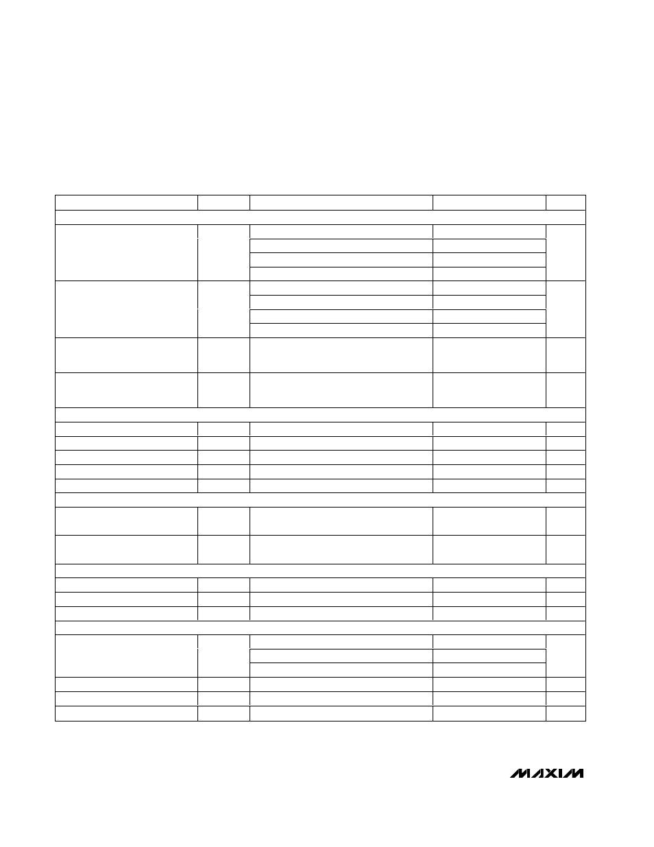
ELECTRICAL CHARACTERISTICS (continued)
(AV
DD
= DV
DD
= CV
DD
= 3V, AGND = DGND = CGND = 0, f
DAC
= 165Msps, no interpolation, external reference, V
REF
= 1.2V,
I
FS
= 20mA, output amplitude = 0dB FS, differential output, T
A
= T
MIN
to T
MAX
, unless otherwise noted. T
A
> +25°C guaranteed by
production test. T
A
< +25°C guaranteed by design and characterization. Typical values are at T
A
= +25°C.)
PARAMETER
SYMBOL
CONDITIONS
MIN
TYP
MAX
UNITS
INTERPOLATION FILTER (4x interpolation)
-0.005dB
0.200
-0.01dB
0.201
-0.1dB
0.210
Passband Width
f
OUT
/
0.5f
DAC
-3dB
0.239
MHz/
MHz
0.302f
DAC
/ 2 to 1.698f
DAC
/ 2
74
0.300f
DAC
/ 2 to 1.700f
DAC
/ 2
63
0.297f
DAC
/ 2 to 1.703 f
DAC
/ 2
53
Stopband Rejection
0.266f
DAC
/ 2 to 1.734f
DAC
/ 2
14
dB
Group Delay
22
Data
clock
cycles
Impulse Response Duration
27
Data
clock
cycles
LOGIC INPUTS (IDE,
CW, REN, DA9–DA0, DB9–DB0)
Digital Input-Voltage High
V
IH
2
V
Digital Input-Voltage Low
V
IL
0.8
V
Digital Input-Current High
I
H
V
IH
= 2V
-1
+1
µA
Digital Input-Current Low
I
IL
V
IL
= 0.8V
-1
+1
µA
Digital Input Capacitance
C
IN
3
pF
DIGITAL OUTPUTS (CLK)
Digital Output-Voltage High
V
OH
I
SOURCE
= 0.5mA, Figure 1
0.9
×
DV
DD
V
Digital Output-Voltage Low
V
OL
I
SINK
= 0.5mA, Figure 1
0.1
×
DV
DD
V
DIFFERENTIAL CLOCK INPUT (CLKXP, CLKXN)
Clock Input Internal Bias
CV
DD
/ 2
V
Differential Clock Input Swing
0.5
V
P-P
Clock Input Impedance
Single-ended clock drive
5
k
Ω
TIMING CHARACTERISTICS
No interpolation
165
2x interpolation
150
Input Data Rate
f
DATA
4x interpolation
75
Msps
Output Settling Time
t
s
To ±0.1% error band (Note 2)
11
ns
Output Rise Time
10% to 90% (Note 2)
2.5
ns
Output Fall Time
90% to 10% (Note 2)
2.5
ns