Max7313, Functional overview, Pin description – Rainbow Electronics MAX7313 User Manual
Page 6
MAX7313
Functional Overview
The MAX7313 is a general-purpose input/output (GPIO)
peripheral that provides 16 I/O ports, P0–P15, con-
trolled through an I
2
C-compatible serial interface. A
17th output-only port, INT/O16, can be configured as
an interrupt output or as a general-purpose output port.
All output ports sink loads up to 50mA connected to
external supplies up to 5.5V, independent of the
MAX7313’s supply voltage. The MAX7313 is rated for a
ground current of 350mA, allowing all 17 outputs to sink
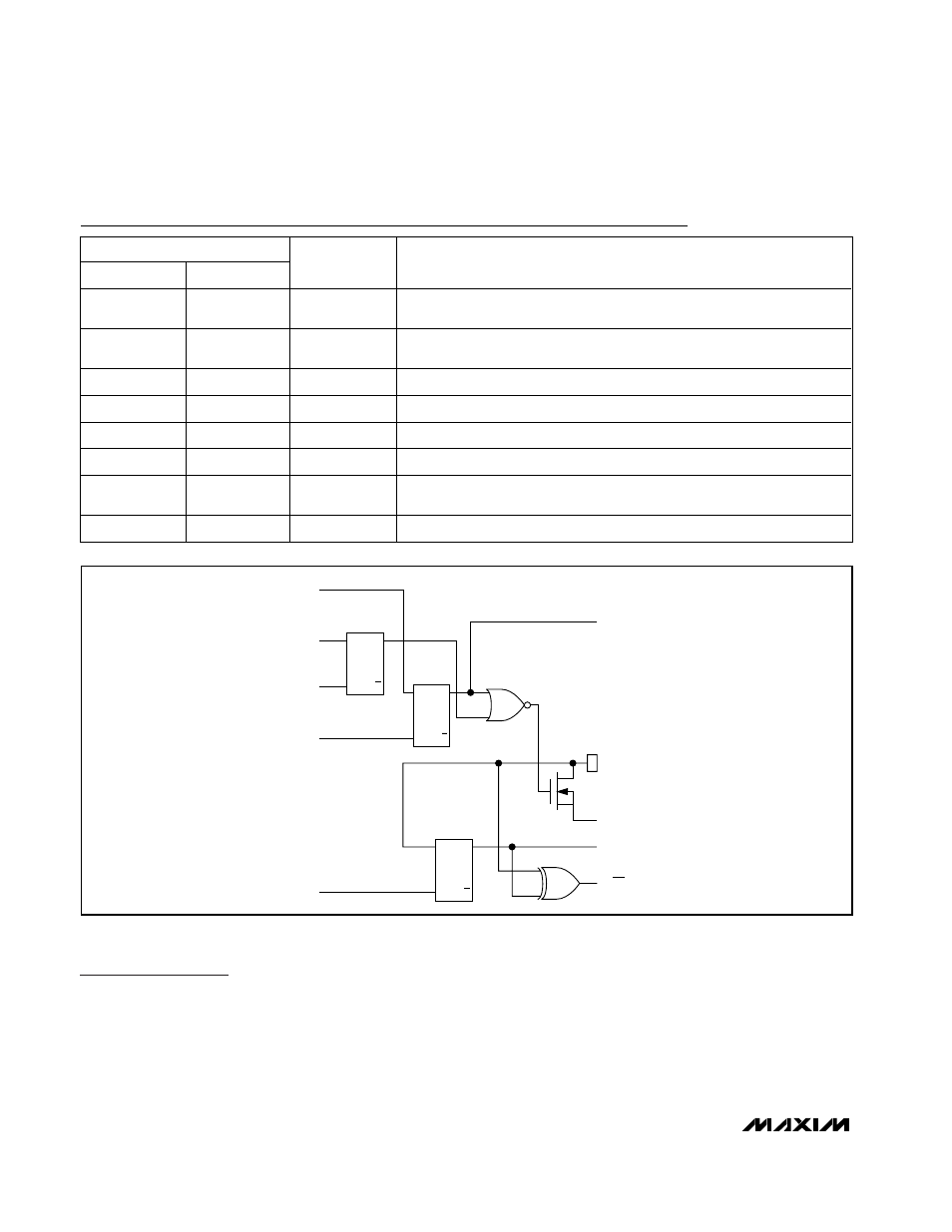
20mA at the same time. Figure 1 shows the output
structure of the MAX7313. The ports default to inputs on
power-up.
Port Inputs and Transition Detection
Input ports registers reflect the incoming logic levels of
the port pins, regardless of whether the pin is defined
16-Port I/O Expander with LED Intensity
Control and Interrupt
6
_______________________________________________________________________________________
Pin Description
Figure 1. Simplified Schematic of I/O Ports
D
C
K
Q
Q
FF
DATA FROM
SHIFT REGISTER
DATA FROM
SHIFT REGISTER
WRITE
CONFIGURATION
PULSE
WRITE PULSE
READ PULSE
CONFIGURATION
REGISTER
D
C
K
Q
Q
FF
INPUT PORT
REGISTER
D
C
K
Q
Q
FF
OUTPUT
PORT
REGISTER
OUTPUT PORT
REGISTER DATA
I/O PIN
Q2
GND
INPUT PORT
REGISTER DATA
TO INT
PIN
QSOP
QFN
NAME
FUNCTION
1
22
INT/O16
Output Port. Open-drain output rated at 7V, 50mA. Configurable as interrupt
output or general-purpose output.
21, 2, 3
18, 23, 24
AD0, AD1,
AD2
Address Inputs. Sets device slave address. Connect to either GND, V+,
SCL, or SDA to give 64 logic combinations. See Table 1.
4–11, 13–20
1–8, 10–17
P0–P15
Input/Output Ports. P0–P15 are open-drain I/Os rated at 5.5V, 50mA.
12
9
GND
Ground. Do not sink more than 350mA into the GND pin.
22
19
SCL
I
2
C-Compatible Serial Clock Input
23
20
SDA
I
2
C-Compatible Serial Data I/O
24
21
V+
Positive Supply Voltage. Bypass V+ to GND with a 0.047µF ceramic
capacitor.
—
PAD
EXPOSED PAD
Exposed pad on package underside. Connect to GND.