Max7313, Chip information, Pin configurations (continued) – Rainbow Electronics MAX7313 User Manual
Page 24: Driving load currents higher than 50ma, Power-supply considerations
MAX7313
where:
R
LED
is the resistance of the resistor in series with the
LED (
Ω).
V
SUPPLY
is the supply voltage used to drive the LED (V).
V
LED
is the forward voltage of the LED (V).
V
OL
is the output low voltage of the MAX7313 when
sinking I
LED
(V).
I
LED
is the desired operating current of the LED (A).
For example, to operate a 2.2V red LED at 14mA from a
5V supply, R
LED
= (5 - 2.2 - 0.25) / 0.014 = 182
Ω.
Driving Load Currents Higher than 50mA
The MAX7313 can be used to drive loads drawing more
than 50mA, like relays and high-current white LEDs, by
paralleling outputs. Use at least one output per 50mA of
load current; for example, a 5V 330mW relay draws
66mA and needs two paralleled outputs to drive it.
Ensure that the paralleled outputs chosen are controlled
by the same blink phase register, i.e., select outputs
from the P0 through P7 range, or the P8 through P15
range. This way, the paralleled outputs are turned on
and off together. Do not use output O16 as part of a
load-sharing design. O16 cannot be switched at the
same time as any of the other outputs because it is con-
trolled by a different register.
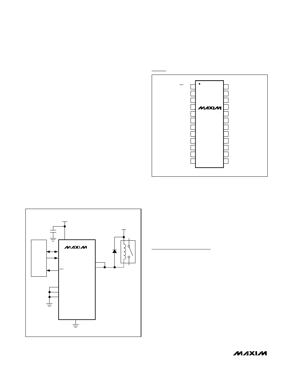
The MAX7313 must be protected from the negative
voltage transient generated when switching off induc-
tive loads, such as relays, by connecting a reverse-
biased diode across the inductive load (Figure 18). The
peak current through the diode is the inductive load’s
operating current.
Power-Supply Considerations
The MAX7313 operates with a power-supply voltage of
2V to 3.6V. Bypass the power supply to GND with at
least 0.047µF as close to the device as possible.
Chip Information
TRANSISTOR COUNT: 25,991
TECHNOLOGY: BiCMOS
16-Port I/O Expander with LED Intensity
Control and Interrupt
24
______________________________________________________________________________________
Figure 18. Diode-Protected Switching Inductive Load
MAX7313
P8
P10
P0
P1
P2
P3
P4
P5
P6
P7
V+
2V TO 3.6V
µC
SDA
SCL
SDA
I/O
AD0
P11
P12
P13
P14
P15
SCL
P9
GND
AD2
AD1
0.047
µF
INT/O16
BAS16
5V
24
23
22
21
20
19
18
17
1
2
3
4
5
6
7
8
V+
SDA
SCL
AD0
P0
AD2
AD1
TOP VIEW
P15
P14
P13
P12
P4
P3
P2
P1
16
15
14
13
9
10
11
12
P11
P10
P9
P8
GND
P7
P6
P5
QSOP
MAX7313AEG
INT/O16
Pin Configurations (continued)