Max7315, Functional overview, Pin description – Rainbow Electronics MAX7315 User Manual
Page 6
MAX7315
Functional Overview
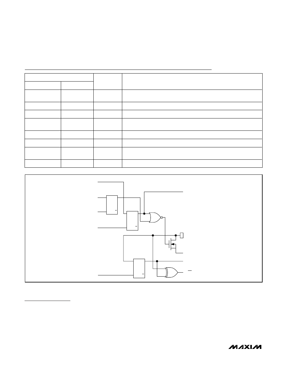
The MAX7315 is a general-purpose input/output (GPIO)
peripheral that provides eight I/O ports, P0–P7, con-
trolled through an I
2
C-compatible serial interface. A 9th
output-only port, INT/O8, can be configured as an inter-
rupt output or as a general-purpose output port. All out-
put ports sink loads up to 50mA connected to external
supplies up to 5.5V, independent of the MAX7315’s
supply voltage. The MAX7315 is rated for a ground cur-
rent of 190mA, allowing all nine outputs to sink 20mA at
the same time. Figure 1 shows the output structure of
the MAX7315. The ports default to inputs on power-up.
Port Inputs and Transition Detection
An input ports register reflects the incoming logic levels
of the port pins, regardless of whether the pin is
defined as an input or an output. Reading the input
8-Port I/O Expander with LED Intensity
Control and Interrupt
6
_______________________________________________________________________________________
PIN
QSOP/TSSOP
QFN
NAME
FUNCTION
1, 2, 3
15, 16, 1
AD0, AD1,
AD2
Address Inputs. Sets device slave address. Connect to either GND, V+,
SCL, or SDA to give 64 logic combinations. See Table 1.
4–7, 9–12
2–5, 7–10
P0–P7
Input/Output Ports. P0–P7 are open-drain I/Os rated at 5.5V, 50mA.
8
6
GND
Ground. Do not sink more than 190mA into the GND pin.
13
11
INT/O8
Output Port. Open-drain output rated at 7.0V, 50mA. Configurable as
interrupt output or general-purpose output.
14
12
SCL
I
2
C-Compatible Serial Clock Input
15
13
SDA
I
2
C-Compatible Serial Data I/O
16
14
V+
Positive Supply Voltage. Bypass V+ to GND with a 0.047µF ceramic
capacitor
—
PAD
Exposed pad
Exposed Pad on Package Underside. Connect to GND.
Pin Description
Figure 1. Simplified Schematic of I/O Ports
D
C
K
Q
Q
FF
DATA FROM
SHIFT REGISTER
DATA FROM
SHIFT REGISTER
WRITE
CONFIGURATION
PULSE
WRITE PULSE
READ PULSE
CONFIGURATION
REGISTER
D
C
K
Q
Q
FF
INPUT PORT
REGISTER
D
C
K
Q
Q
FF
OUTPUT
PORT
REGISTER
OUTPUT PORT
REGISTER DATA
I/O PIN
Q2
GND
INPUT PORT
REGISTER DATA
TO INT