Applications information, Table 8. blink phase 0 register, Table 9. blink phase 1 register – Rainbow Electronics MAX7315 User Manual
Page 17
Using PWM Intensity Controls with Blink Enabled
When blink is enabled (Table 7), the blink phase 0 regis-
ter and blink phase 1 register specify each output’s logic
level during the PWM on-time during the respective blink
phases (Tables 8 and 9). The effect of setting an output’s
blink phase X register bit to 0 or 1 is shown in Table 12.
LEDs can be flipped between either directly on and off,
or between a variety of high/low PWM intensities.
Global/O8 Intensity Control
The 4 bits used for output O8’s PWM individual intensity
setting also double as the global intensity control
(Table 13). Global intensity simplifies the PWM settings
when the application requires them all to be the same,
such as for backlight applications, by replacing the 9
individual settings with 1 setting. Global intensity is
enabled with the global intensity flag G in the configu-
ration register (Table 4). When global PWM control is
used, the 4 bits of master intensity and 4 bits of O8
intensity effectively combine to provide an 8 bit, 240-
step intensity control applying to all outputs.
It is not possible to apply global PWM control to a sub-
set of the ports, and use the others as logic outputs. To
mix static logic outputs and PWM outputs, individual
PWM control must be selected (Table 10).
Applications Information
Output Level Translation
The open-drain output architecture allows the ports to
level translate the outputs to higher or lower voltages
than the MAX7315 supply. An external pullup resistor
can be used on any output to convert the high-imped-
ance logic-high condition to a positive voltage level.
The resistor can be connected to any voltage up to
5.5V. For interfacing CMOS inputs, a pullup resistor
value of 220k
Ω is a good starting point. Use a lower
resistance to improve noise immunity, in applications
where power consumption is less critical, or where a
faster rise time is needed for a given capacitive load.
Compatibility with PCA9534 and
PCA9554(A)
The MAX7315 is pin compatible and software compatible
with PCA9534, and its variants PCA9554 and
PCA9554A. However, some PCA9534 and PCA9554(A)
functions are not implemented in the MAX7315, and the
MAX7315's PWM and blink functionality is not supported
in the PCA9534 and PCA9554(A). Software compatibility
is clearly not 100%, but the MAX7315 was designed so
the subset (omitted) features default to the same power-
up behavior as the PCA9534 and PCA9554(A), and the
superset features do not use existing registers in a differ-
ent way. In practice, many applications can use the
MAX7315 as a drop-in replacement for the PCA9534 or
PCA9554(A) with no software change.
Driving LED Loads
When driving LEDs, a resistor in series with the LED
must be used to limit the LED current to no more than
50mA. Choose the resistor value according to the fol-
lowing formula:
R
LED
= (V
SUPPLY
- V
LED
- V
OL
) / I
LED
where:
R
LED
is the resistance of the resistor in series with the
LED (
Ω).
V
SUPPLY
is the supply voltage used to drive the LED (V).
V
LED
is the forward voltage of the LED (V).
MAX7315
8-Port I/O Expander with LED Intensity
Control and Interrupt
______________________________________________________________________________________
17
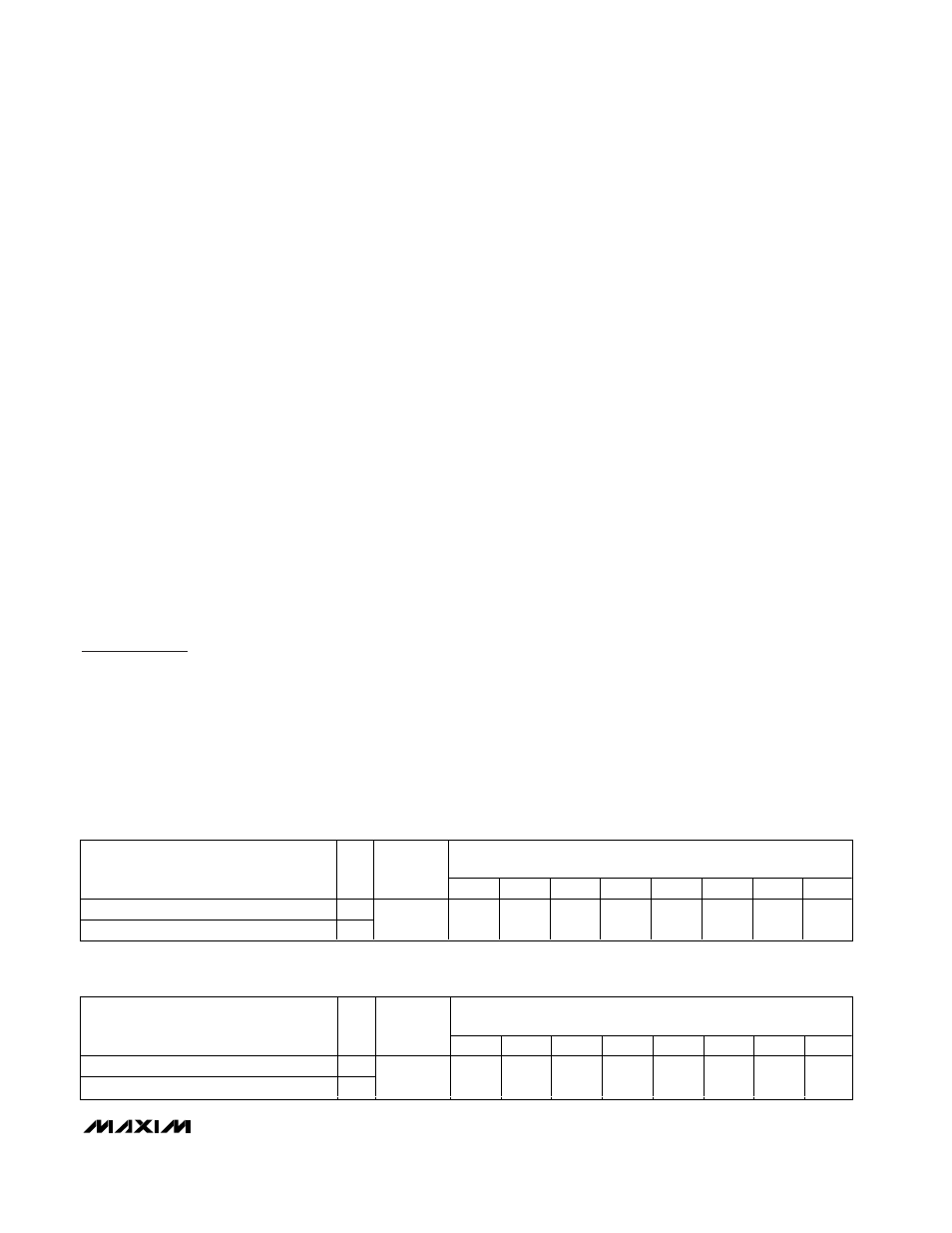
Table 8. Blink Phase 0 Register
REGISTER DATA
REGISTER
R/
W
ADDRESS
CODE
(HEX)
D7
D6
D5
D4
D3
D2
D1
D0
Write outputs phase 0
0
Read-back outputs phase 0
1
0x01
OP7
OP6
OP5
OP4
OP3
OP2
OP1
OP0
Table 9. Blink Phase 1 Register
REGISTER DATA
REGISTER
R/
W
ADDRESS
CODE
(HEX)
D7
D6
D5
D4
D3
D2
D1
D0
Write outputs phase 1
0
Read-back outputs phase 1
1
0x09
OP7
OP6
OP5
OP4
OP3
OP2
OP1
OP0