Max7315, Detailed description, Command address autoincrementing – Rainbow Electronics MAX7315 User Manual
Page 12: Device reset, Initial power-up, Configuration register
MAX7315
Command Address Autoincrementing
The command address stored in the MAX7315 circu-
lates around grouped register functions after each data
byte is written or read (Table 2).
Device Reset
If a device reset input is needed, consider the
MAX7316. The MAX7316 includes a RST input, which
clears any transaction to or from the MAX7316 on the
serial interface and configures the internal registers to
the same state as a power-up reset.
Detailed Description
Initial Power-Up
On power-up all control registers are reset and the
MAX7315 enters standby mode (Table 3). Power-up
status makes all ports into inputs and disables both the
PWM oscillator and blink functionality.
Configuration Register
The configuration register is used to configure the PWM
intensity mode, interrupt, and blink behavior, operate
the INT/O8 output, and read back the interrupt status
(Table 4).
8-Port I/O Expander with LED Intensity
Control and Interrupt
12
______________________________________________________________________________________
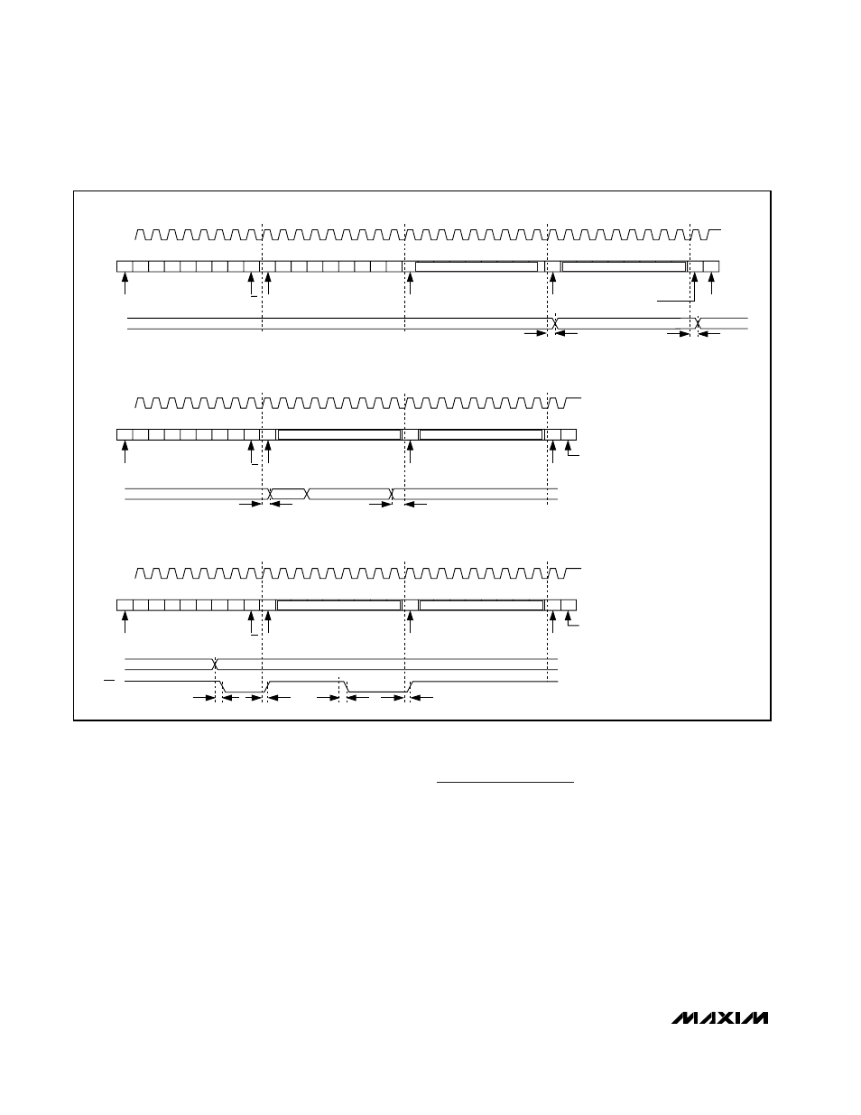
Figure 10. Read, Write, and Interrupt Timing Diagrams
SLAVE ADDRESS
1
2
3
4
5
6
7
8
9
S A6 A5 A4 A3 A2 A1 A0
0
A
0
0
0
0
0
0
0
COMMAND BYTE
1
A
A
A
P
START CONDITION
ACKNOWLEDGE FROM SLAVE
ACKNOWLEDGE FROM SLAVE
ACKNOWLEDGE FROM SLAVE
STOP
CONDITION
P7–P0
DATA1 VALID
DATA2 VALID
SLAVE ADDRESS
1
2
3
4
5
6
7
8
9
S A6 A5 A4 A3 A2 A1 A0
1
A
COMMAND BYTE
A
NA
START CONDITION
ACKNOWLEDGE FROM SLAVE
ACKNOWLEDGE FROM MASTER
P7–P0
STOP CONDITION
P
NO ACKNOWLEDGE FROM
MASTER
DATA2
DATA3
t
DV
t
DV
SLAVE ADDRESS
1
2
3
4
5
6
7
8
9
S A6 A5 A4 A3 A2 A1 A0 1
A
COMMAND BYTE
A
NA
START CONDITION
ACKNOWLEDGE FROM SLAVE
ACKNOWLEDGE FROM MASTER
P7–P0
STOP CONDITION
P
NO ACKNOWLEDGE FROM
MASTER
DATA1
DATA2
DATA3
DATA4
t
DH
t
DS
DATA1
t
IV
t
IR
t
IR
t
IV
SCL
SDA
SCL
SDA
SCL
SDA
WRITE TO OUTPUT PORTS REGISTERS (BLINK PHASE 0 REGISTERS/BLINK PHASE 1 REGISTERS)
READ FROM INPUT PORTS REGISTERS
INTERRUPT VALID/RESET
R/W
MSB
LSB
DATA1
MSB
LSB
DATA1
MSB
LSB
DATA2
MSB
LSB
DATA4
MSB
LSB
DATA4
MSB
LSB
DATA2
R/W
R/W
INT