Absolute maximum ratings, Electrical characteristics – Rainbow Electronics MAX9755 User Manual
Page 2
MAX9750/MAX9751/MAX9755
2.6W Stereo Audio Power Amplifiers and
DirectDrive Headphone Amplifiers
2
_______________________________________________________________________________________
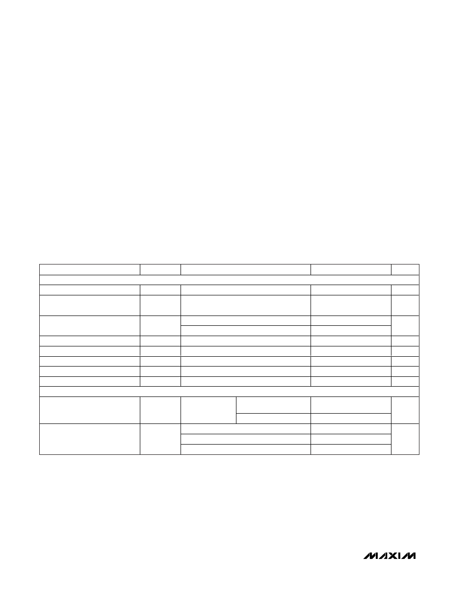
ABSOLUTE MAXIMUM RATINGS
Stresses beyond those listed under “Absolute Maximum Ratings” may cause permanent damage to the device. These are stress ratings only, and functional
operation of the device at these or any other conditions beyond those indicated in the operational sections of the specifications is not implied. Exposure to
absolute maximum rating conditions for extended periods may affect device reliability.
Supply Voltage (V
DD
, PV
DD
, HPV
DD
, CPV
DD
to GND)..........+6V
GND to PGND.....................................................................±0.3V
CPV
SS
, C1N, V
SS
to GND .........................-6.0V to (GND + 0.3V)
HPOUT_ to GND ....................................................................±3V
Any Other Pin .............................................-0.3V to (V
DD
+ 0.3V)
Duration of OUT_ Short Circuit to GND or PV
DD
........Continuous
Duration of OUT_+ Short Circuit to OUT_- .................Continuous
Duration of HPOUT_ Short Circuit to GND,
V
SS
or HPV
DD
.........................................................Continuous
Continuous Current (PV
DD
, OUT_, PGND) ...........................1.7A
Continuous Current (CPV
DD
, C1N, C1P, CPV
SS
, V
SS
, HPV
DD
,
HPOUT_) .......................................................................850mA
Continuous Input Current (All Other Pins) ........................±20mA
Continuous Power Dissipation (T
A
= +70°C)
28-Pin Thin QFN (derate 20.8mW/°C above +70°C) ..1667mW
28-Pin TSSOP (derate 13mW/°C above +70°C) .........1039mW
Junction Temperature ......................................................+150°C
Operating Temperature Range ...........................-40°C to +85°C
Storage Temperature Range .............................-65°C to +150°C
Lead Temperature (soldering, 10s) .................................+300°C
ELECTRICAL CHARACTERISTICS
(V
DD
= PV
DD
= CPV
DD
= HPV
DD
= 5V, GND = PGND = CPGND = 0V,
SHDN = V
DD
, C
BIAS
= 1µF, C1 = C2 = 1µF, speaker load
terminated between OUT_+ and OUT_-, headphone load terminated between HPOUT_ and GND, GAIN1 = GAIN2 = VOL = GAIN = 0V,
T
A
= T
MIN
to T
MAX
, unless otherwise noted. Typical values are at T
A
= +25°C.) (Note 1)
PARAMETER
SYMBOL
CONDITIONS
MIN
TYP
MAX
UNITS
GENERAL
Supply Voltage Range
V
DD
, PV
DD
Inferred from PSRR test
4.5
5.5
V
Headphone Supply Voltage
CPV
DD
,
HPV
DD
Inferred from PSRR test
3
5.5
V
HPS = GND, speaker mode, R
L
=
∞
14
29
Quiescent Supply Current
I
DD
HPS = V
DD
, headphone mode, R
L
=
∞
7
13
mA
Shutdown Supply Current
I
SHDN
SHDN = GND
0.2
5
µA
Bias Voltage
V
BIAS
1.7
1.8
1.9
V
Switching Time
t
SW
Gain or input switching
10
µs
Input Resistance
R
IN
Amplifier inputs (Note 2)
10
20
30
k
Ω
Turn-On Time
t
SON
25
ms
SPEAKER AMPLIFIER (HPS = GND)
MAX9750A/MAX9750B/
MAX9751/MAX9755
±
1
±
15
Output Offset Voltage
V
OS
Measured
between OUT_+
and OUT_-
MAX9750C
±
0.4
±
6
mV
PV
DD
or V
DD
= 4.5V to 5.5V (T
A
= +25
°C)
75
90
f = 1kHz, V
RIPPLE
= 200mV
P-P
80
Power-Supply Rejection Ratio
(Note 3)
PSRR
f = 10kHz, V
RIPPLE
= 200mV
P-P
55
dB