Electrical characteristics (continued) – Rainbow Electronics MAX12553 User Manual
Page 6
MAX12553
14-Bit, 65Msps, 3.3V ADC
6
_______________________________________________________________________________________
Note 1:
Specifications ≥+25°C guaranteed by production test; <+25°C guaranteed by design and characterization.
Note 2:
See definitions in the Parameter Definitions section at the end of this data sheet.
Note 3:
Specifications guaranteed by design and characterization. Devices tested for performance during production test.
Note 4:
During power-down, D13–D0, DOR, and DAV are high impedance.
Note 5:
Guaranteed by design and characterization.
Note 6:
Digital outputs settle to V
IH
or V
IL
.
Note 7:
Due to test-equipment-jitter limitations at 175MHz, 0.15% of the spectrum on each side of the fundamental is excluded from
the spectral analysis.
Note 8:
Limit specifications include performance degradations due to a production test socket. Performance is improved when the
MAX12553 is soldered directly to the PC board.
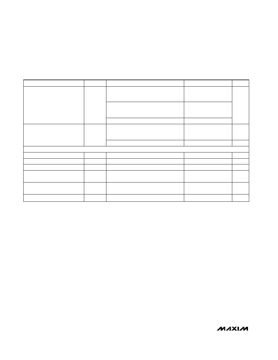
ELECTRICAL CHARACTERISTICS (continued)
(V
DD
= 3.3V, OV
DD
= 2.0V, GND = 0, REFIN = REFOUT (internal reference), V
IN
= -0.5dBFS, CLKTYP = high, DCE = high, PD = low,
G/T = low, f
CLK
= 65MHz (50% duty cycle), T
A
= -40°C to +85°C, unless otherwise noted. Typical values are at T
A
= +25°C.) (Note 1)
PARAMETER
SYMBOL
CONDITIONS
MIN
TYP
MAX
UNITS
Normal operating mode,
f
IN
= 175MHz at -0.5dBFS, CLKTYP = GND,
single-ended clock
337
Normal operating mode,
f
IN
= 175MHz at -0.5dBFS,
CLKTYP = OV
DD
, differential clock
363
406
Analog Power Dissipation
P
DISS
Power-down mode clock idle, PD = OV
DD
0.15
mW
Normal operating mode,
f
IN
= 175MHz at -0.5dBFS, OV
DD
= 2.0V,
C
L
≈
5pF
8.2
mA
Digital Output Supply Current
I
OVDD
Power-down mode clock idle, PD = OV
DD
20
µA
TIMING CHARACTERISTICS (Figure 6)
Clock Pulse-Width High
t
CH
7.7
ns
Clock Pulse-Width Low
t
CL
7.7
ns
Data-Valid Delay
t
DAV
C
L
= 5pF (Note 6)
6.9
ns
Data Setup Time Before Rising
Edge of DAV
t
SETUP
C
L
= 5pF (Notes 5, 6)
8.5
ns
Data Hold Time After Rising Edge
of DAV
t
HOLD
C
L
= 5pF (Notes 5, 6)
6.3
ns
Wake-Up Time from Power-Down
t
WAKE
V
REFIN
= 2.048V
10
ms