Bit, 65msps, 3.3v adc, Detailed description, Input track-and-hold (t/h) circuit – Rainbow Electronics MAX12553 User Manual
Page 14: Reference output (refout)
MAX12553
Detailed Description
The MAX12553 uses a 10-stage, fully differential,
pipelined architecture (Figure 1) that allows for high-
speed conversion while minimizing power consump-
tion. Samples taken at the inputs move progressively
through the pipeline stages every half-clock cycle.
From input to output, the total clock-cycle latency is 8.5
clock cycles.
Each pipeline converter stage converts its input voltage
into a digital output code. At every stage, except the
last, the error between the input voltage and the digital
output code is multiplied and passed along to the next
pipeline stage. Digital error correction compensates for
ADC comparator offsets in each pipeline stage and
ensures no missing codes. Figure 2 shows the
MAX12553 functional diagram.
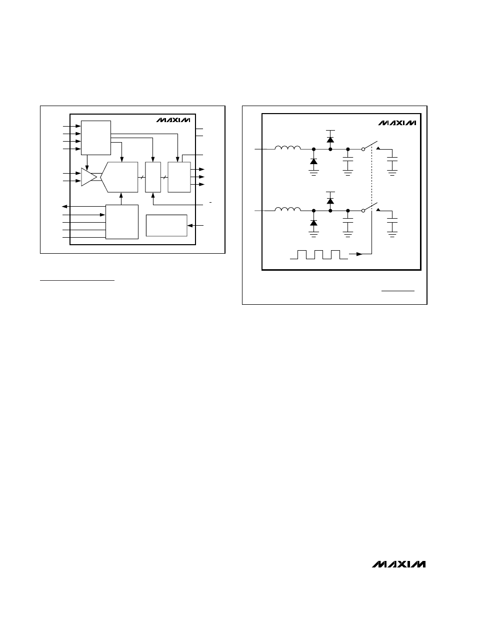
Input Track-and-Hold (T/H) Circuit
Figure 3 displays a simplified functional diagram of the
input T/H circuit. This input T/H circuit allows for high
analog input frequencies of 175MHz and beyond and
supports a common-mode input voltage of V
DD
/2 ±0.5V.
The MAX12553 sampling clock controls the ADC’s
switched-capacitor T/H architecture (Figure 3) allowing
the analog input signal to be stored as charge on the
sampling capacitors. These switches are closed (track)
when the sampling clock is high and open (hold) when
the sampling clock is low (Figure 4). The analog input
signal source must be capable of providing the dynam-
ic current necessary to charge and discharge the sam-
pling capacitors. To avoid signal degradation, these
capacitors must be charged to one-half LSB accuracy
within one-half of a clock cycle.
The analog input of the MAX12553 supports differential
or single-ended input drive. For optimum performance
with differential inputs, balance the input impedance of
INP and INN and set the common-mode voltage to mid-
supply (V
DD
/2). The MAX12553 provides the optimum
common-mode voltage of V
DD
/2 through the COM out-
put when operating in internal reference mode and
buffered external reference mode. This COM output
voltage can be used to bias the input network as shown
in Figures 10, 11, and 12.
Reference Output (REFOUT)
An internal bandgap reference is the basis for all the
internal voltages and bias currents used in the
MAX12553. The power-down logic input (PD) enables
and disables the reference circuit. The reference circuit
requires 10ms to power up and settle when power is
applied to the MAX12553 or when PD transitions from
high to low. REFOUT has approximately 17kΩ to GND
when the MAX12553 is in power-down.
The internal bandgap reference and its buffer generate
V
REFOUT
to be 2.048V. The reference temperature coeffi-
cient is typically +50ppm/°C. Connect an external ≥0.1µF
bypass capacitor from REFOUT to GND for stability.
14-Bit, 65Msps, 3.3V ADC
14
______________________________________________________________________________________
MAX12553
INP
INN
14-BIT
PIPELINE
ADC
DEC
REFERENCE
SYSTEM
COM
REFOUT
REFN
REFP
OV
DD
DAV
OUTPUT
DRIVERS
D13–D0
DOR
REFIN
T/H
POWER CONTROL
AND
BIAS CIRCUITS
CLKP
CLOCK
GENERATOR
AND
DUTY-CYCLE
EQUALIZER
CLKN
CLKTYP
PD
V
DD
GND
DCE
G/T
Figure 2. Simplified Functional Diagram
MAX12553
C
PAR
2pF
V
DD
BOND WIRE
INDUCTANCE
1.5nH
INP
SAMPLING
CLOCK
*THE EFFECTIVE RESISTANCE OF THE
SWITCHED SAMPLING CAPACITORS IS:
*C
SAMPLE
4.5pF
C
PAR
2pF
V
DD
BOND WIRE
INDUCTANCE
1.5nH
INN
*C
SAMPLE
4.5pF
R
SAMPLE
=
1
f
CLK
x C
SAMPLE
Figure 3. Simplified Input T/H Circuit