Pin description – Rainbow Electronics MAX12553 User Manual
Page 12
MAX12553
14-Bit, 65Msps, 3.3V ADC
12
______________________________________________________________________________________
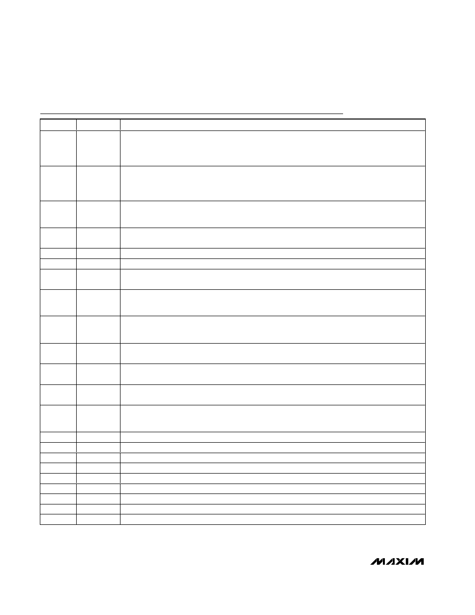
PIN
NAME
FUNCTION
1
REFP
Positive Reference I/O. The full-scale analog input range is
±
(V
REFP
- V
REFN
) x 2/3. Bypass REFP to
GND with a 0.1µF capacitor. Connect a 1µF capacitor in parallel with a 10µF capacitor between REFP
and REFN.
Place the 1µF REFP to REFN capacitor as close to the device as possible on the same
side of the PC board.
2
REFN
Negative Reference I/O. The full-scale analog input range is
±
(V
REFP
- V
REFN
) x 2/3. Bypass REFN to
GND with a 0.1µF capacitor. Connect a 1µF capacitor in parallel with a 10µF capacitor between REFP
and REFN.
Place the 1µF REFP to REFN capacitor as close to the device as possible on the same
side of the PC board.
3
COM
Common-Mode Voltage I/O. Bypass COM to GND with a 2.2µF capacitor.
Place the 2.2µF COM to
GND capacitor as close to the device as possible
. This 2.2µF capacitor can be placed on the
opposite side of the PC board and connected to the MAX12553 through a via.
4, 7, 16,
35
GND
Ground. Connect all ground pins and EP together.
5
INP
Positive Analog Input
6
INN
Negative Analog Input
8
DCE
Duty-Cycle Equalizer Input. Connect DCE low (GND) to disable the internal duty-cycle equalizer.
Connect DCE high (OV
DD
or V
DD
) to enable the internal duty-cycle equalizer.
9
CLKN
Negative Clock Input. In differential clock input mode (CLKTYP = OV
DD
or V
DD
), connect the differential
clock signal between CLKP and CLKN. In single-ended clock mode (CLKTYP = GND), apply the single-
ended clock signal to CLKP and connect CLKN to GND.
10
CLKP
Positive Clock Input. In differential clock input mode (CLKTYP = OV
DD
or V
DD
), connect the differential
clock signal between CLKP and CLKN. In single-ended clock mode (CLKTYP = GND), apply the single-
ended clock signal to CLKP and connect CLKN to GND.
11
CLKTYP
Clock Type Definition Input. Connect CLKTYP to GND to define the single-ended clock input. Connect
CLKTYP to OV
DD
or V
DD
to define the differential clock input.
12–15, 36
V
DD
Analog Power Input. Connect V
DD
to a 3.15V to 3.60V power supply. Bypass V
DD
to GND with a parallel
capacitor combination of
≥
2.2µF and 0.1µF. Connect all V
DD
pins to the same potential.
17, 34
OV
DD
Output-Driver Power Input. Connect OV
DD
to a 1.7V to V
DD
power supply. Bypass OV
DD
to GND with a
parallel capacitor combination of
≥
2.2µF and 0.1µF.
18
DOR
Data Out-of-Range Indicator. The DOR digital output indicates when the analog input voltage is out of
range. When DOR is high, the analog input is beyond its full-scale range. When DOR is low, the analog
input is within its full-scale range (Figure 6).
19
D13
CMOS Digital Output, Bit 13 (MSB)
20
D12
CMOS Digital Output, Bit 12
21
D11
CMOS Digital Output, Bit 11
22
D10
CMOS Digital Output, Bit 10
23
D9
CMOS Digital Output, Bit 9
24
D8
CMOS Digital Output, Bit 8
25
D7
CMOS Digital Output, Bit 7
26
D6
CMOS Digital Output, Bit 6
27
D5
CMOS Digital Output, Bit 5
Pin Description