Electrical characteristics—max5176 (continued) – Rainbow Electronics MAX5176 User Manual
Page 5
MAX5174/MAX5176
Low-Power, Serial, 12-Bit DACs
with Voltage Output
_______________________________________________________________________________________
5
Note 1:
INL guaranteed between codes 10 and 4095.
Note 2:
Offset is measured at the code that comes closest to 10mV.
Note 3:
Accuracy is better than 1 LSB for V
OUT
= 10mV to V
DD
- 180mV. Guaranteed by PSR test on end points.
Note 4:
R
L
= open and digital inputs are either V
DD
or DGND.
Note 5:
INL guaranteed between codes 20 and 4095.
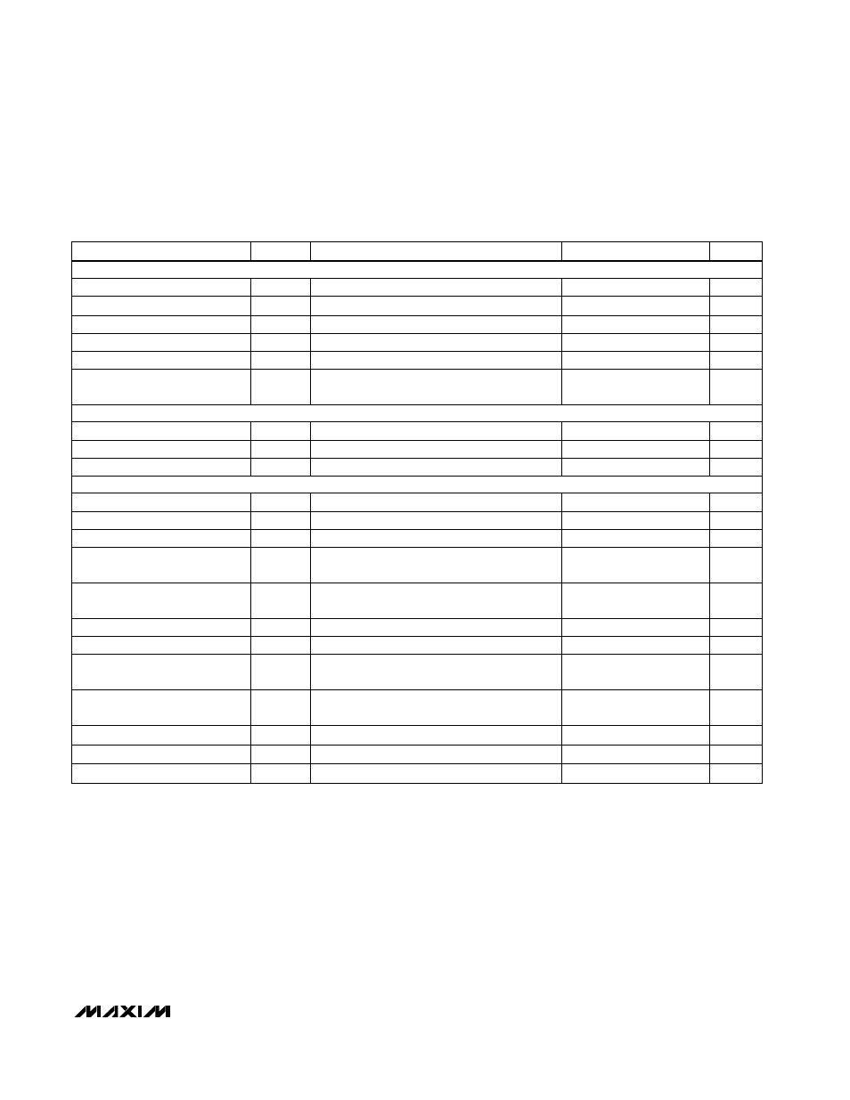
ELECTRICAL CHARACTERISTICS—MAX5176 (continued)
(V
DD
= +2.7V to +3.6V, V
REF
= 1.25V, OS = AGND = DGND, R
L
= 5k
Ω
, C
L
= 100pF referenced to ground, T
A
= T
MIN
to T
MAX
, unless
otherwise noted. Typical values are at T
A
= +25°C).
Power-Supply Current (Note 4)
I
DD
0.35
0.4
mA
Positive Supply Voltage
V
DD
2.7
3.6
V
Digital Feedthrough
1
nV-s
CS = V
DD
, DIN = 50kHz; f
SCLK
= 100kHz,
V
SCLK
= 3Vp-p
PARAMETER
SYMBOL
MIN
TYP
MAX
UNITS
Time Required to Exit Shutdown
40
µs
OS Pin Input Resistance
80
120
k
Ω
Output Voltage Swing (Note 3)
0 V
DD
V
Voltage Output Slew Rate
SR
0.6
V/µs
CS Pulse Width High
t
CSW
150
ns
SCLK Rise to CS Fall Delay
t
CS0
10
ns
Output Settling Time
18
µs
To ±0.5LSB, from 10mV to full-scale
SCLK Fall to DOUT Valid
Propagation Delay
t
DO2
200
ns
C
LOAD
= 200pF
CS Rise to SCLK Rise Hold Time
t
CS1
75
ns
SCLK Rise to DOUT Valid
Propagation Delay
t
DO1
200
ns
C
LOAD
= 200pF
SDI Hold Time
t
DH
0
ns
SDI Setup Time
t
DS
60
ns
SCLK Rise to CS Rise Hold Time
t
CSH
0
ns
CSB
Fall to SCLK Rise Setup
Time
t
CSS
60
ns
SCLK Pulse Width Low
t
CL
CONDITIONS
75
ns
SCLK Pulse Width High
t
CH
75
ns
SCLK Clock Period
t
CP
150
ns
Shutdown Current (Note 4)
1
10
µA
DYNAMIC PERFORMANCE
POWER SUPPLIES
TIMING CHARACTERISTICS