Applications information, User-programmable logic output (upo), Reset (rs) and clear ( clr ) – Rainbow Electronics MAX5176 User Manual
Page 12: Unipolar output, Bipolar output
MAX5174/MAX5176
Low-Power, Serial, 12-Bit DACs
with Voltage Output
12
______________________________________________________________________________________
User-Programmable Logic Output (UPO)
The user-programmable logic output (UPO) allows con-
trol of an external device through the serial interface,
thereby reducing the number of microcontroller I/O pins
required. During power-down, this output will retain its
digital state prior to shutdown. When CLR is pulled low,
UPO will reset to its programmed default state. See
Table 1 for specific commands to control the UPO.
Reset (RS) and Clear (
CLR)
The MAX5174/MAX5176 offers a clear pin (CLR), which
resets the output voltage. If RS = DGND, then CLR
resets the output voltage to 0. If RS = V
DD
, then CLR
resets the output voltage to mid-scale. In either case,
CLR will reset UPO to its programmed default state.
Applications Information
Unipolar Output
Figure 6 shows the MAX5174/MAX5176 configured for
unipolar, rail-to-rail operation with a gain of 1.638V/V.
Table 2 lists the codes for unipolar output voltages. The
output voltage is limited to V
DD
. Use the OS pin to intro-
duce an offset voltage as shown in Figure 7 and
described in the
Offset and Buffer Configurations
section.
Bipolar Output
Figure 8 shows the MAX5174/MAX5176 configured for
bipolar output operation. The output voltage is given by
the following equation (OS = AGND):
where N represents the numeric value of the DAC’s
binary input code and V
REF
is the voltage of the exter-
nal reference. Table 3 shows digital codes and the cor-
responding output voltage for Figure 8’s circuit.
V
V
N
OUT
REF
=
⋅
−
2
4096
1
CS
SCLK
DIN
COMMAND
EXECUTED
9
8
16
1
C1
C2
S0
C0
D9
D8
D7
D6
D3
D2
D1
D0
S2
S1
D5
D4
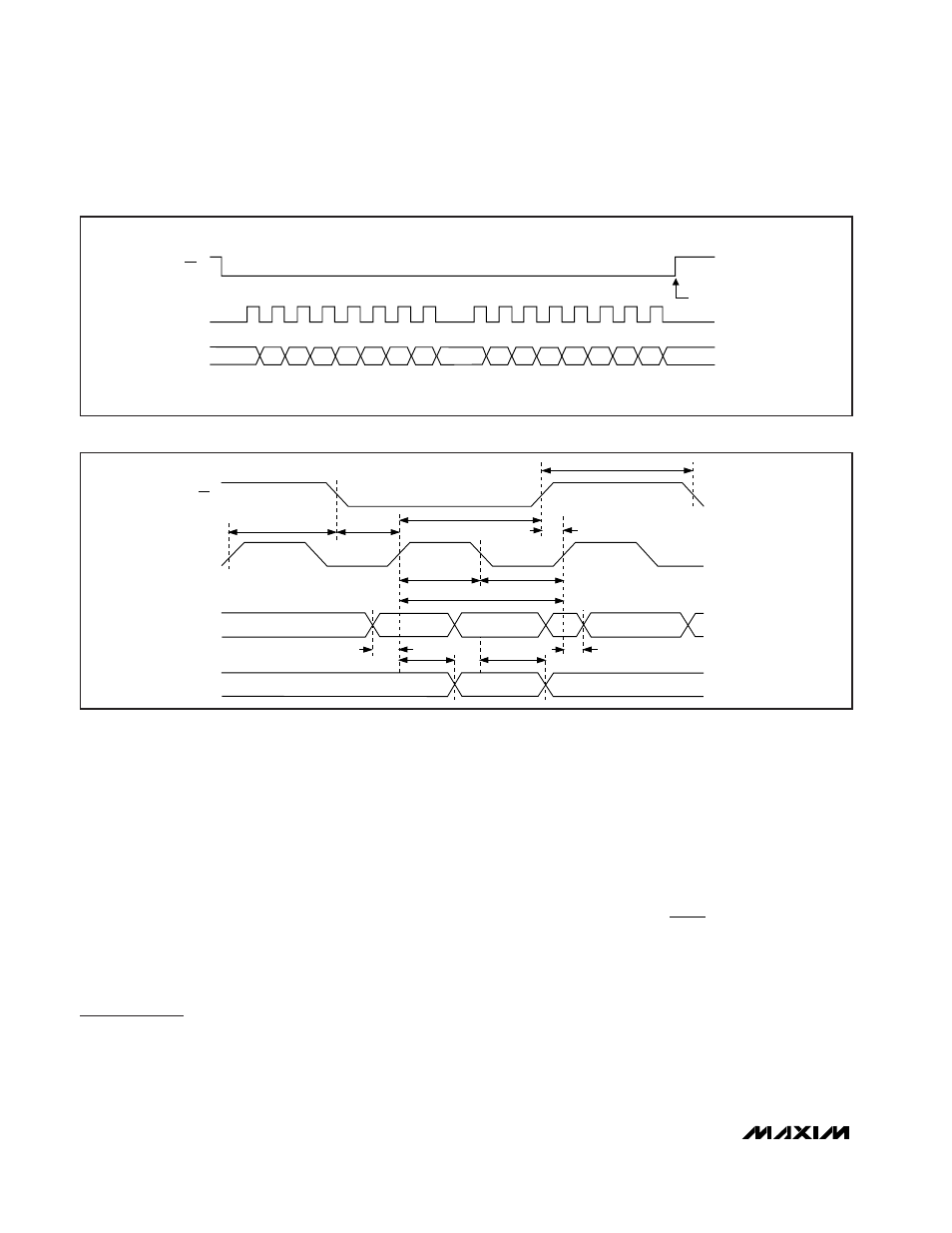
Figure 4. Serial-Interface Timing Diagram
CS
SCLK
DIN
DOUT
t
CSW
t
CS1
t
CSH
t
CSS
t
CSO
t
D02
t
CH
t
CL
t
CP
t
D01
t
DS
t
DH
Figure 5. Detailed Serial-Interface Timing Diagram