Using an ac reference, Power-supply and layout considerations – Rainbow Electronics MAX5176 User Manual
Page 14
MAX5174/MAX5176
Low-Power, Serial, 12-Bit DACs
with Voltage Output
14
______________________________________________________________________________________
TO OTHER
SERIAL DEVICES
MAX5174
MAX5176
DIN
SCLK
CS
MAX5174
MAX5176
MAX5174
MAX5176
DIN
DOUT
DOUT
DOUT
SCLK
CS
DIN
SCLK
CS
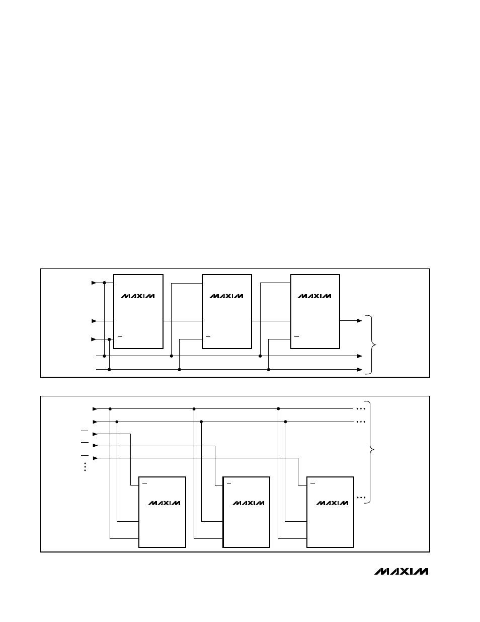
Figure 9. Daisy-Chaining MAX5174/MAX5175 Devices
TO OTHER
SERIAL DEVICES
MAX5174
MAX5176
DIN
SCLK
CS
MAX5174
MAX5176
DIN
SCLK
CS
MAX5174
MAX5176
DIN
SCLK
CS
DIN
SCLK
CS1
CS2
CS3
Figure 10. Multiple MAX5174/MAX5176s Sharing Common DIN and SCLK Lines
Using an AC Reference
The MAX5174/MAX5176 accept references with AC
components, as long as the reference voltage remains
between 0 and V
DD
- 1.4V. Figure 11 shows a tech-
nique for applying a sine-wave signal to the reference
input where the AC signal is offset before being applied
to REF. The reference voltage must remain above
AGND.
Power-Supply and Layout Considerations
Wire-wrap boards are not recommended. For optimum
system performance, use printed circuit boards with
separate analog and digital ground planes. Connect
the two ground planes together at the low-impedance
power-supply source. Connect DGND and AGND pins
together at the IC. The best ground connection is
achieved by connecting the DAC’s DGND and AGND
pins together and connecting that point to the system
analog ground plane. This is useful because if the
DAC’s DGND is connected to the system digital
ground, digital noise may infiltrate the DAC’s analog
portion.
Bypass the power supply with a 4.7µF capacitor in par-
allel with a 0.1µF capacitor to AGND. Minimize capaci-
tor lead lengths to reduce inductance. If noise
becomes an issue, use shielding and/or ferrite beads to
increase isolation.
To maintain INL and DNL performance as well as gain
drift, it is extremely important to provide the lowest pos-
sible reference output impedance at the DAC reference
input pin. INL degrades if the series resistance on REF
pin exceeds 0.1
Ω
. The same consideration must be
made for the AGND pin.