Table 1. serial-interface programming commands – Rainbow Electronics MAX5176 User Manual
Page 11
MAX5174/MAX5176
Low-Power, Serial, 12-Bit DACs
with Voltage Output
______________________________________________________________________________________
11
The MAX5174/MAX5176 accepts one 16-bit packet or
two 8-bit packets sent while CS remains low. The
MAX5174/MAX5176 allow the following to be config-
ured:
• Clock edge on which serial data output (DOUT) is
clocked.
• State of the user-programmable logic output.
• Configuration of the reset state.
Specific commands for setting these are shown in
Table 1.
The general timing diagram in Figure 4 illustrates how
the MAX5174/MAX5176 acquires data. CS must go low
at least t
CSS
before the rising edge of the serial clock
(SCLK). With CS low, data is clocked into the register
on the rising edge of SCLK. The maximum serial clock
frequency guaranteed for proper operation is 10MHz
for the MAX5174 and 6MHz for the MAX5176. See
Figure 5 for a detailed timing diagram of the serial inter-
face.
Serial Data Output (DOUT)
The serial-data output (DOUT) is the internal shift regis-
ter’s output and allows for daisy-chaining of multiple
devices as well as data readback (see
Applications
Information
). By default upon start-up, data shifts out of
DOUT on the serial clock’s rising edge (Mode 0) and
provides a lag of 16 clock cycles, thus maintaining SPI,
QSPI, and MICROWIRE compatibility. However, if the
device is programmed for Mode 1, then the output data
lags DIN by 16.5 clock cycles and is clocked out on the
serial clock’s rising edge. During shutdown, DOUT
retains its last digital state prior to shutdown.
Load input register; DAC registers are updated (start-up DAC with
new data).
1
0
Load input register; DAC registers are unchanged.
0
0
12-bit DAC data
12-bit DAC data
D11..................D0
C1
FUNCTION
C0
No operation (NOP).
1
1
0 0 x x xxxx xxxx
xxxxxxxxxxxx
Update DAC register from input register (start-up DAC with data
previously stored in the input registers).
0
1
UPO goes low (default).
1
1
1 0 0 x xxxx xxxx
0 1 x x xxxx xxxx
Mode 1, DOUT clocked out on SCLK’s rising edge.
1
1
1 1 0 x xxxx xxxx
1 0 1 x xxxx xxxx
UPO goes high.
1
1
Shut down DAC (provided PDL = 1).
1
1
Mode 0, DOUT clocked out on SCLK’s falling edge (default).
1
1
1 1 1 x xxxx xxxx
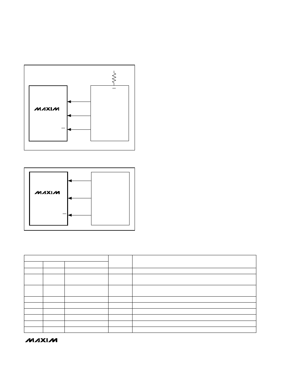
DIN
SCLK
CS
MOSI
SCK
I/O
SPI/QSPI
PORT
SS
+5V
CPOL = 0, CPHA = 0
MAX5174
MAX5176
Figure 2. Connections for SPI and QSPI Standards
SCLK
DIN
CS
SK
SO
I/O
MICROWIRE
PORT
MAX5174
MAX5176
Figure 3. Connections for MICROWIRE
Table 1. Serial-Interface Programming Commands
16-BIT SERIAL WORD
0 0
0 0
S1, S0
xx
xx
xx
xx
xx
xx
xx