Table 2. unipolar code table (circuit of figure 6), Table 3. bipolar code table (circuit of figure 8), Offset and buffer configurations – Rainbow Electronics MAX5176 User Manual
Page 13: Daisy-chaining devices
MAX5174/MAX5176
Low-Power, Serial, 12-Bit DACs
with Voltage Output
Offset and Buffer Configurations
The simple circuit of Figure 7 illustrates how to intro-
duce an offset to the output voltage. The amount of off-
set introduced by a voltage at the OS pin is shown in
the following equation:
V
OFFSET
= V
OS
·
(1- Gain)
where Gain = 1.638.
However, the total output voltage of the device cannot
exceed V
DD
, regardless of the voltage on the OS pin.
To set the gain of the output amplifier to 1, connect OS
to OUT.
Daisy-Chaining Devices
The serial-data output pin (DOUT) allows multiple
MAX5174/MAX5176s to be daisy-chained together as
shown in Figure 9. The advantage of this is that only two
lines are needed to control all the DACs. The disadvan-
tage is that it takes
n
commands to program the DACs.
Figure 10 shows several MAX5174/MAX5176s sharing
one common DIN signal line. In this configuration the
data bus is common to all devices; however, more I/O
lines are required because each device needs a dedi-
cated CS line. The advantage of this configuration is
that only one command is needed to program any DAC.
DAC CONTENTS
MSB
LSB
11 1111 1111 11 (00)
10 0000 0000 01 (00)
+V
REF
(2049/4096)
·
1.638
+V
REF
(4095/4096)
·
1.638
ANALOG OUTPUT
10 0000 0000 00 (00)
+V
REF
(2048/4096)
·
1.638
01 1111 1111 11 (00)
+V
REF
(2047/4096)
·
1.638
00 0000 0000 01 (00)
+V
REF
(1/4096)
·
1.638
00 0000 0000 00 (00)
0
Table 2. Unipolar Code Table
(Circuit of Figure 6)
MAX5174
MAX5176
DAC
REF
OUT
OS
DGND
AGND
+5V/+3V
V
DD
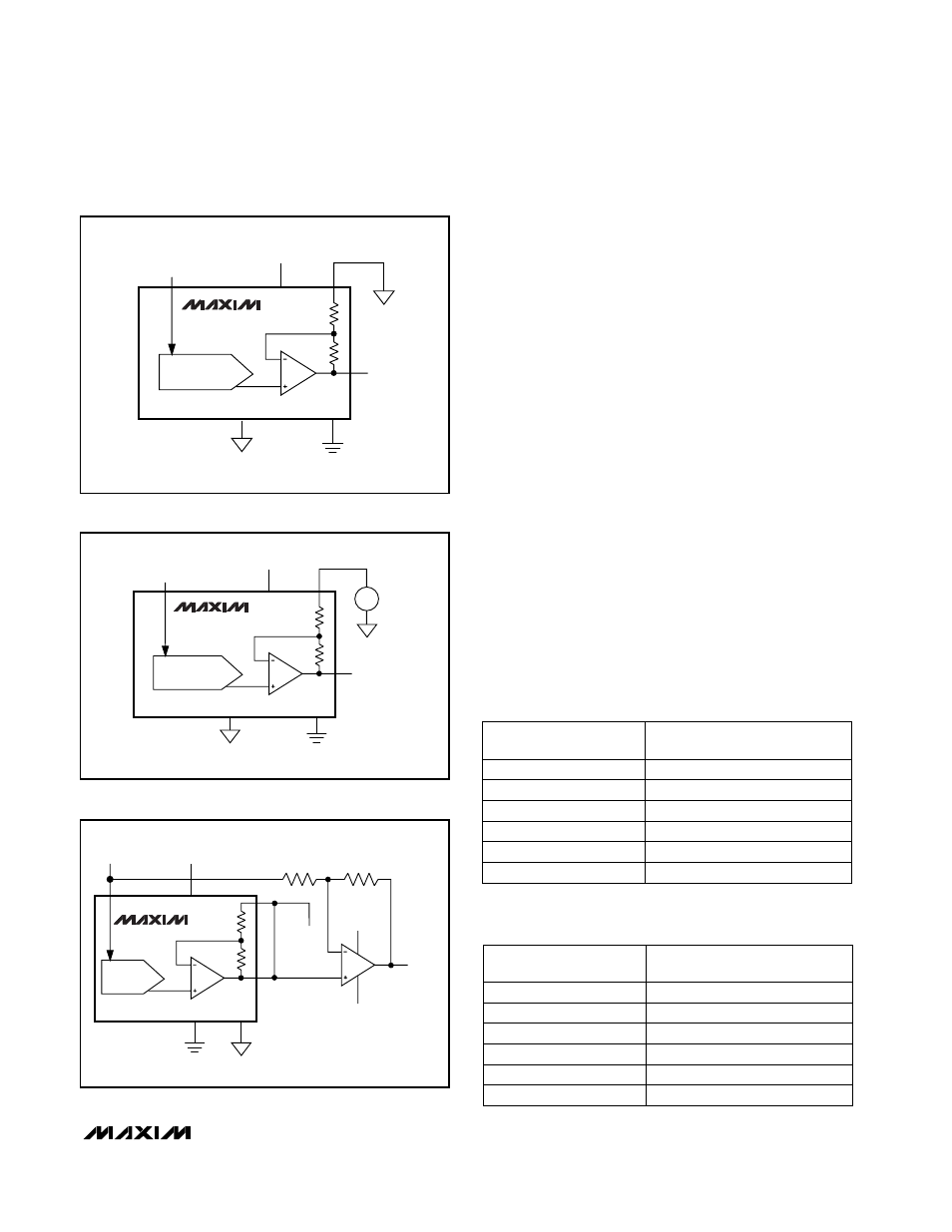
Figure 6. Unipolar Output Circuit (Rail-to-Rail)
DAC CONTENTS
MSB
LSB
11 1111 1111 11 (00)
10 0000 0000 01 (00)
+V
REF
[(2 · 2049/4096) - 1]
+V
REF
[(2 · 4095/4096) - 1]
ANALOG OUTPUT
01 1111 1111 11 (00)
+V
REF
[(2 · 2047/4096) - 1]
00 0000 0000 01 (00)
+V
REF
[(2 · 1/4096) - 1]
10 0000 0000 00 (00)
+V
REF
[(2 · 2048/4096) - 1]
00 0000 0000 00 00
-V
REF
Table 3. Bipolar Code Table
(Circuit of Figure 8)
Figure 7. Setting OS for Output Offset
MAX5174
MAX5176
DAC
AGND
DGND
REF
OUT
OS
V
OS
+5V/+3V
V
DD
________________________________________________________________________________________13
TOLERANCES: 10k
Ω
±0.1%
AGND
DGND
MAX5174
MAX5176
DAC
REF
OS
OUT
10k
10k
V-
V+
V
DD
V
OUT
+5V/+3V
Figure 8. Bipolar Output Circuit