Pin description – Rainbow Electronics MAX16831 User Manual
Page 8
MAX16831
High-Voltage, High-Power LED Driver with
Analog and PWM Dimming Control
8
_______________________________________________________________________________________
8
_______________________________________________________________________________________
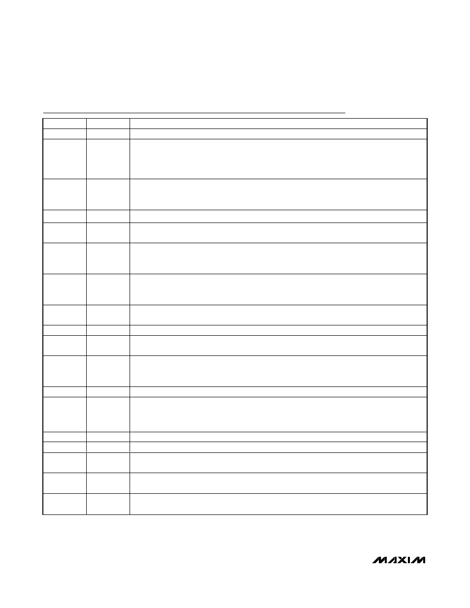
Pin Description
PIN
NAME
FUNCTION
1, 24
N.C.
No Connection. Not internally connected.
2
UVEN
Undervoltage Lockout (UVLO) Threshold/Enable Input. UVEN is a dual-function adjustable UVLO
threshold input with an enable feature. Connect UVEN to V
CC
through a resistive voltage-divider to
program the UVLO threshold. Connect UVEN directly to V
CC
to use the 6.0V (max) default UVLO
threshold. Apply a voltage greater than 1.244V to UVEN to enable the device.
3
REG1
5V Regulator Output. REG1 is an internal low-dropout voltage regulator that generates a 5V (V
CC
>
6V) output voltage and supplies power to internal circuitry. Bypass REG1 to AGND through a 1µF
ceramic capacitor.
4
AGND
Analog Ground
5
REF
Accurate 3V Buffered Reference Output. Connect REF to DIM through a resistive voltage-divider to
apply a DC voltage for analog-controlled dimming functionality. Leave REF unconnected if unused.
6
DIM
Dimming Control Input. Connect DIM to an external PWM signal for PWM dimming. For analog-
controlled dimming, connect DIM to REF through a resistive voltage-divider. The dimming frequency
is 200Hz under these conditions. Connect DIM to AGND to turn off the LEDs.
7
RTSYNC
SYNC Input/Output. The PWM clock is generated by the RTSYNC oscillator. Connect an external
resistor to RTSYNC to select a clock switching frequency from 125kHz to 600kHz or connect RTSYNC
to an external clock to synchronize the MAX16831 with a master clock signal.
8
CLKOUT
Clock Output. CLKOUT buffers the oscillator/clock. Connect CLKOUT to the SYNC input of another
device to operate the MAX16831 in a multichannel configuration. CLKOUT is a logic output.
9, 10, 11
I.C.
Internally Connected. Must be connected to AGND.
12
COMP
Error-Amplifier Output. Connect the compensation network from COMP to FB for stable closed-loop
control. Use low-leakage ceramic capacitors in the feedback network.
13
CS
Current-Sense Amplifier Output. The current-sense amplifier (CSA) senses the differential voltage
across the load sense resistor, R
CS
, and generates a voltage, V
CS
, at CS proportional to the LED
current. Connect the proper compensation resistor from CS to FB.
14
FB
Error-Amplifier Inverting Input
15
OV
Overvoltage Protection Input. Connect OV to HI through a resistive voltage-divider to set the
overvoltage limit for the load. When the voltage at OV exceeds the 1.235V (typ) threshold, an
overvoltage fault is generated and the switching MOSFET turns off. The MOSFET is turned on again
when the voltage at OV drops below 1.17V (typ).
16, 17
SGND
Switching Ground. SGND is the ground for non-analog and high-current gate driver circuitry.
18
DRV
Gate Driver Output. Connect DRV to the gate of an external n-channel MOSFET for switching.
19
DRI
Gate Driver Supply Input. Connect DRI to REG2 to power the primary switching MOSFET driver.
Bypass DRI to AGND through a 10µF ceramic capacitor.
20
SNS+
Positive Peak Current-Sense Input. Connect SNS+ to the positive side of the switch current-sense
resistor, R
SENSE
.
21
SNS-
Negative Peak Current-Sense Input. Connect SNS- to the negative side of the switch current-sense
resistor, R
SENSE
.