Applications information, Table 1. functional table, Table 2. transmitter mode – Rainbow Electronics SCAN92LV090 User Manual
Page 7: Table 3. receiver mode, Test circuits and timing waveforms, Figure 1. differential driver dc test circuit, Figure 1
Applications Information
General application guidelines and hints may be found in the
following application notes: AN-808, AN-1108, AN-977,
AN-971, and AN-903.
There are a few common practices which should be implied
when designing PCB for Bus LVDS signaling. Recom-
mended practices are:
•
Use at least 4 PCB board layer (Bus LVDS signals,
ground, power and TTL signals).
•
Keep drivers and receivers as close to the (Bus LVDS
port side) connector as possible.
•
Bypass each Bus LVDS device and also use distributed
bulk capacitance between power planes. Surface mount
capacitors placed close to power and ground pins work
best. Two or three high frequency, multi-layer ceramic
(MLC) surface mount (0.1 µF, 0.01 µF, 0.001 µF) in
parallel should be used between each V
CC
and ground.
The capacitors should be as close as possible to the V
CC
pin.
Multiple vias should be used to connect V
CC
and Ground
planes to the pads of the by-pass capacitors.
In addition, randomly distributed by-pass capacitors
should be used.
•
Use the termination resistor which best matches the dif-
ferential impedance of your transmission line.
•
Leave unused Bus LVDS receiver inputs open (floating).
Limit traces on unused inputs to
<
0.5 inches.
•
Isolate TTL signals from Bus LVDS signals
MEDIA (CONNECTOR or BACKPLANE) SELECTION:
•
Use controlled impedance media. The backplane and
connectors should have a matched differential imped-
ance.
TABLE 1. Functional Table
MODE SELECTED
DE
RE
DRIVER MODE
H
H
RECEIVER MODE
L
L
TRI-STATE MODE
L
H
LOOP BACK MODE
H
L
TABLE 2. Transmitter Mode
INPUTS
OUTPUTS
DE
D
IN
DO+
DO−
H
L
L
H
H
H
H
L
H
0.8V
<
D
IN
<
2.0V
X
X
L
X
Z
Z
TABLE 3. Receiver Mode
INPUTS
OUTPUT
RE
(RI+) – (RI−)
L
L (
<
−100 mV)
L
L
H (
>
+100 mV)
H
L
−100 mV
<
V
ID
<
+100 mV
X
H
X
Z
X = High or Low logic state
L = Low state
Z = High impedance state
H = High state
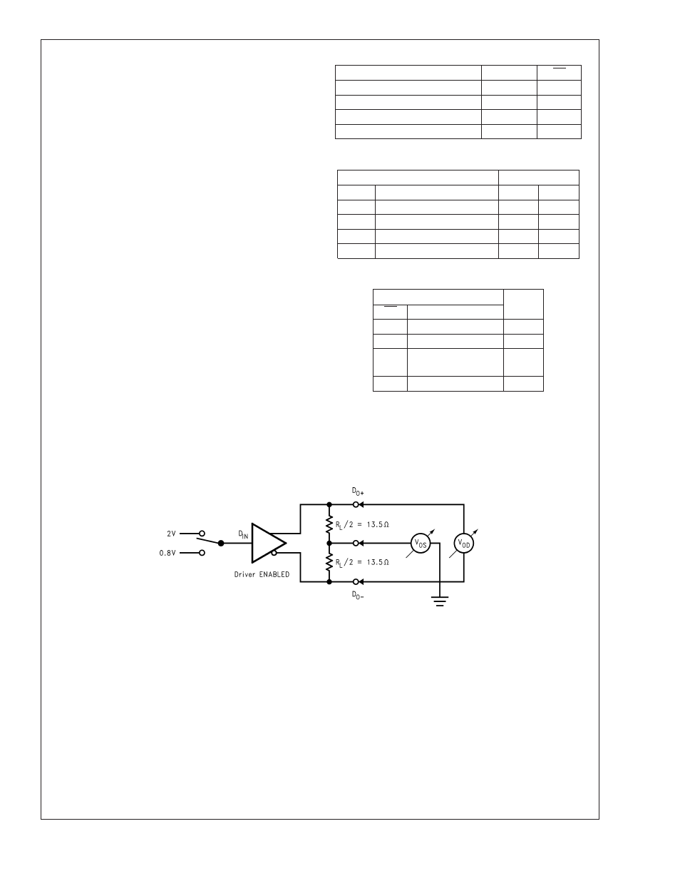
Test Circuits and Timing Waveforms
10124203
FIGURE 1. Differential Driver DC Test Circuit
SCAN92L
V090
www.national.com
7