Note 6)(20, Note 10), Note 11) – Rainbow Electronics SCAN92LV090 User Manual
Page 6: Note, Note 6), Note 8), Note 9), Note 12), Note 13), Ac electrical characteristics
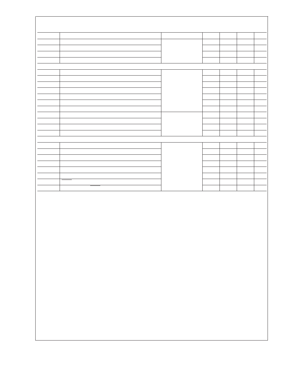
AC Electrical Characteristics
(Continued)
Over recommended operating supply voltage and temperature ranges unless otherwise specified (Note 6)
Symbol
Parameter
Conditions
Min
Typ
Max
Units
t
PHZ
Disable Time High to Z
R
L
= 27
Ω,
C
L
= 10 pF
3
8
ns
t
PLZ
Disable Time Low to Z
3
8
ns
t
PZH
Enable Time Z to High
3
8
ns
t
PZL
Enable Time Z to Low
3
8
ns
DIFFERENTIAL RECEIVER TIMING REQUIREMENTS
t
PHLD
Differential Prop. Delay High to Low (Note 8)
C
L
= 35 pF
2.0
2.4
3.9
ns
t
PLHD
Differential Prop Delay Low to High (Note 8)
2.0
2.4
3.9
ns
t
SDK1
Differential Skew |t
PHLD
–t
PLHD
| (Note 9)
210
ps
t
SDK2
Chip to Chip Skew (Note 12)
1.9
ns
t
SDK3
Channel to Channel skew (Note 13)
0.35
0.7
ns
t
TLH
Transition Time Low to High
1.5
2.5
ns
t
THL
Transition Time High to Low
1.5
2.5
ns
t
PHZ
Disable Time High to Z
R
L
= 500
Ω,
C
L
= 35 pF
4.5
10
ns
t
PLZ
Disable Time Low to Z
3.5
8
ns
t
PZH
Enable Time Z to High
3.5
8
ns
t
PZL
Enable Time Z to Low
3.5
8
ns
SCAN CIRCUITRY TIMING REQUIREMENTS
f
MAX
Maximum TCK Clock Frequency
R
L
= 500
Ω, C
L
= 35
pF
25.0
75.0
MHz
t
S
TDI to TCK, H or L
1.5
ns
t
H
TDI to TCK, H or L
1.5
ns
t
S
TMS to TCK, H or L
2.5
ns
t
H
TMS to TCK, H or L
1.5
ns
t
W
TCK Pulse Width, H or L
10.0
ns
t
W
TRST Pulse Width, L
2.5
ns
t
REC
Recovery Time, TRST to TCK
2.0
ns
Note 1: “Absolute Maximum Ratings” are those values beyond which the safety of the device cannot be guaranteed. They are not meant to imply that the devices
should be operated at these limits. The table of “Electrical Characteristics” provides conditions for actual device operation.
Note 2: All currents into device pins are positive; all currents out of device pins are negative. All voltages are referenced to ground unless otherwise specified except
V
OD
,
∆V
OD
and V
ID
.
Note 3: All typicals are given for V
CC
= +3.3V and T
A
= +25˚C, unless otherwise stated.
Note 4: ESD Rating: HBM (1.5 k
Ω, 100 pF)
>
4.5 kV EIAJ (0
Ω, 200 pF)
>
300V.
Note 5: C
L
includes probe and fixture capacitance.
Note 6: Generator waveforms for all tests unless otherwise specified: f = 25 MHz, Z
O
= 50
Ω, t
r
, t
f
=
<
1.0 ns (0%–100%). To ensure fastest propagation delay and
minimum skew, data input edge rates should be equal to or faster than 1ns/V; control signals equal to or faster than 3ns/V. In general, the faster the input edge rate,
the better the AC performance.
Note 7: The DS92LV090A functions within datasheet specification when a resistive load is applied to the driver outputs.
Note 8: Propagation delays are guaranteed by design and characterization.
Note 9: t
SKD1
|t
PHLD
–t
PLHD
| is the worse case skew between any channel and any device over recommended operation conditions.
Note 10: Only one output at a time should be shorted, do not exceed maximum package power dissipation capacity.
Note 11: V
OH
failsafe terminated test performed with 27
Ω connected between RI+ and RI− inputs. No external voltage is applied.
Note 12: Chip to Chip skew is the difference in differential propagation delay between any channels of any devices, either edge.
Note 13: Channel to Channel skew is the difference in driver output or receiver output propagation delay between any channels within a device, common edge.
SCAN92L
V090
www.national.com
6