Pinout description – Rainbow Electronics SCAN92LV090 User Manual
Page 3
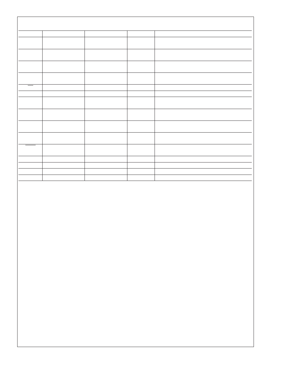
Pinout Description
Pin Name
TQFP Pin #
BGA Pin #
Input/Output
Descriptions
DO+/RI+
27, 31, 35, 37, 41,
45, 47, 51, 55
A7, B8, C6, D5, D8,
E6, F7, G5, G6
I/O
True Bus LVDS Driver Outputs and Receiver Inputs.
DO−/RI−
26, 30, 34, 36, 40,
44, 46, 50, 54
B5, B6, C7, D6, E5,
E8, F6, G8, H7
I/O
Complimentary Bus LVDS Driver Outputs and
Receiver Inputs.
D
IN
2, 6, 12, 18, 20, 22,
58, 60, 62
A2, A4, C3, C4, D2,
E3, G3, G4, H3
I
TTL Driver Input.
RO
3, 7, 13, 19, 21, 23,
59, 61, 63
A3, B3, C1, C2, D4,
E4, F4, G1, H2
O
TTL Receiver Output.
RE
17
H1
I
Receiver Enable TTL Input (Active Low).
DE
16
G2
I
Driver Enable TTL Input (Active High).
GND
4, 5, 9, 14, 25, 56
B1, B4, D3, E1, F2,
H5
Power
Ground for digital circuitry (must connect to GND on
PC board). These pins connected internally.
V
CC
10, 15, 24, 57, 64
A1, A5, F1, F3, H4
Power
V
CC
for digital circuitry (must connect to V
CC
on PC
board). These pins connected internally.
AGND
28, 33, 43, 49, 53
A8, C5, D7, F5, G7
Power
Ground for analog circuitry (must connect to GND
on PC board). These pins connected internally.
AV
CC
29, 32, 42, 48, 52
A6, B7, C8, H6, H8
Power
Analog V
CC
(must connect to V
CC
on PC board).
These pins connected internally.
TRST
39
F8
I
Test Reset Input to support IEEE 1149.1 (Active
Low)
TMS
38
E7
I
Test Mode Select Input to support IEEE 1149.1
TCK
1
B2
I
Test Clock Input to support IEEE 1149.1
TDI
8
D1
I
Test Data Input to support IEEE 1149.1
TDO
11
E2
O
Test Data Output to support IEEE 1149.1
SCAN92L
V090
www.national.com
3