Absolute maximum ratings, Package thermal characteristics, Electrical characteristics – Rainbow Electronics MAX98314 User Manual
Page 3
����������������������������������������������������������������� Maxim Integrated Products 3
MAX98314
Mono 3.2W Class D Amplifier
with Integrated Input Coupling Capacitors
PVDD, IN+, IN-, SHDN, GAIN to PGND ................... 0.3V to +6V
OUT+, OUT- to PGND ............................0.3V to (V
PVDD
+ 0.3V)
Continuous Current In/Out of PVDD, PGND, OUT_ .........750mA
Continuous Input Current (all other pins) ........................ Q20mA
Duration of Short Circuit Between
OUT_ to PVDD, PGND ..........................................Continuous
Between OUT+ and OUT- Pins .............................Continuous
Continuous Power Dissipation (T
A
= +70NC) for Multilayer Board
WLP (derate 10.64mW/NC above +70NC) .....................851mW
Junction Temperature .....................................................+150NC
Operating Temperature Range .......................... -40NC to +85NC
Storage Temperature Range ............................ -65NC to +150NC
Soldering Temperature (reflow) ......................................+260NC
WLP
Junction-to-Ambient Thermal Resistance (B
JA
) ........102NC/W
Junction-to-Case Thermal Resistance (B
JC
) ...............47NC/W
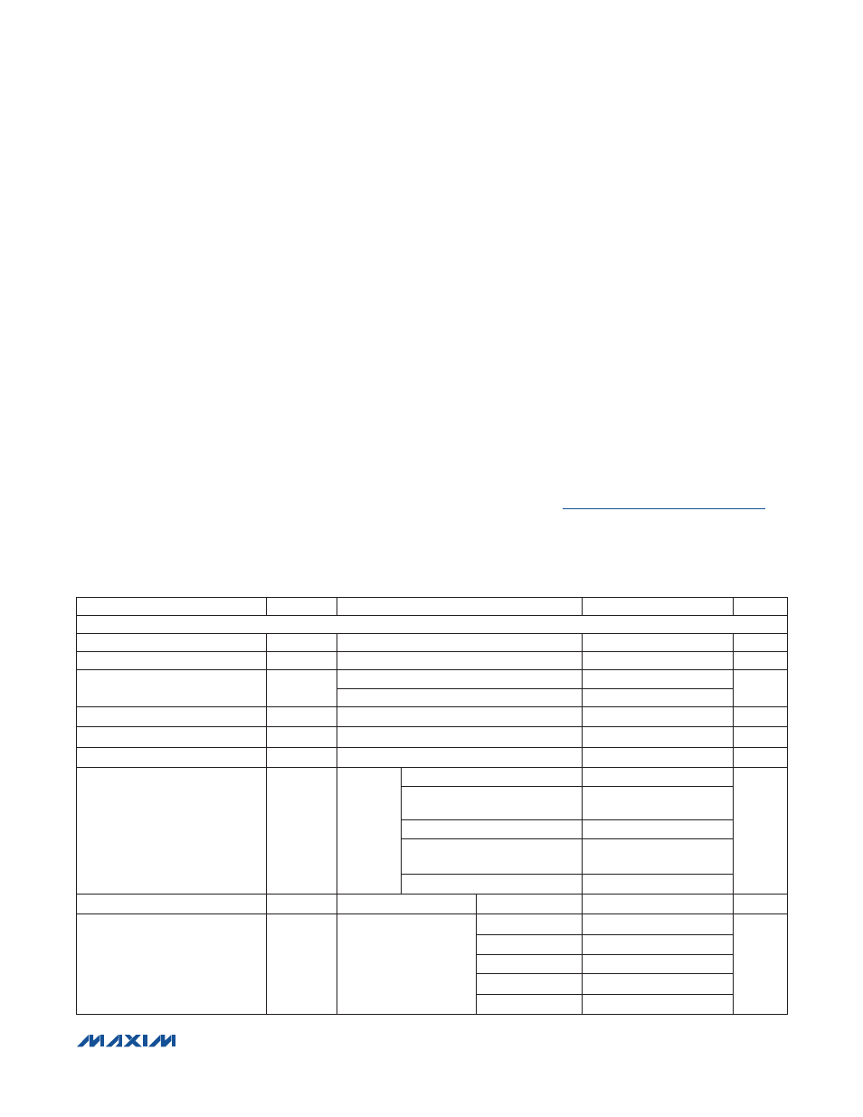
ABSOLUTE MAXIMUM RATINGS
Note 1: Package thermal resistances were obtained using the method described in JEDEC specification JESD51-7, using a four-
layer board. For detailed information on package thermal considerations, refer to
www.maxim-ic.com/thermal-tutorial
.
Stresses beyond those listed under “Absolute Maximum Ratings” may cause permanent damage to the device. These are stress ratings only, and functional opera-
tion of the device at these or any other conditions beyond those indicated in the operational sections of the specifications is not implied. Exposure to absolute
maximum rating conditions for extended periods may affect device reliability.
PACKAGE THERMAL CHARACTERISTICS (Note 1)
ELECTRICAL CHARACTERISTICS
(V
PVDD
= V
SHDN
= V
GAIN
= 5V, V
PGND
= 0V, A
V
= 6dB (GAIN = PVDD), R
L
= J, R
L
connected between OUT+ to OUT-, AC measure-
ment bandwidth 20Hz to 22kHz, T
A
= T
MIN
to T
MAX
, unless otherwise noted. Typical values are at T
A
= +25NC.) (Note 2, 3)
PARAMETER
SYMBOL
CONDITIONS
MIN
TYP
MAX
UNITS
AMPLIFIER CHARACTERISTICS
Supply Voltage Range
V
PVDD
Guaranteed by PSRR test
2.5
5.5
V
Undervoltage Lockout
UVLO
PVDD falling
1.8
2.2
V
Quiescent Current
I
PVDD
V
PVDD
= 5V
1.2
1.8
mA
V
PVDD
= 3.7V
0.95
Shutdown Supply Current
I
SHDN
V
SHDN
= 0V, T
A
= +25NC
< 0.1
10
F
A
Turn-On Time
t
ON
3.7
10
ms
Bias Voltage
V
BIAS
V
PVDD
/2
V
Voltage Gain
A
V
f = 1kHz
GAIN connected to PGND
11.75
12
12.25
dB
GAIN connected to PGND
through 100kI Q5% resistor
8.75
9
9.25
GAIN connected to PVDD
5.75
6
6.25
GAIN connected to PVDD
through 100kI Q5% resistor
2.75
3
3.25
GAIN unconnected
-0.25
0
+0.25
Input Capacitance
C
IN
All gains
0.011
F
F
Highpass Corner Frequency
f
C
-3dB down
A
V
= 12dB
199
Hz
A
V
= 9dB
139
A
V
= 6dB
63
100
189
A
V
= 3dB
70
A
V
= 0dB
50